Wu Jingjing, Tang Xin, Long Fei, Tang Biyu. Effect of O–O bonds on p-type conductivity in Ag-doped ZnO twin grain boundaries*
Project supported by the National Natural Science Foundation of China (Grant No. 11364009) and Natural Science Foundation of Guangxi Province, China (Grant No. 2014GXNSFFA118004).
. Chinese Physics B, 2018, 27(5): 057701
Permissions
Effect of O–O bonds on p-type conductivity in Ag-doped ZnO twin grain boundaries*
Project supported by the National Natural Science Foundation of China (Grant No. 11364009) and Natural Science Foundation of Guangxi Province, China (Grant No. 2014GXNSFFA118004).
Key Laboratory of New Processing Technology for Nonferrous Metal & Materials, Ministry of Education, Guilin University of Technology, Guilin 541004, China
College of Material Science and Engineering, Guilin University of Technology, Guilin 541004, China
School of Chemistry & Chemical Engineering, Guangxi University, Nanning 530004, China
† Corresponding author. E-mail: xtang@glut.edu.cn
Project supported by the National Natural Science Foundation of China (Grant No. 11364009) and Natural Science Foundation of Guangxi Province, China (Grant No. 2014GXNSFFA118004).
Abstract
Based on density functional theory, first-principles calculation is applied to study the electronic properties of undoped and Ag-doped ZnO-Σ7 () twin grain boundaries (GBs). The calculated result indicates that the twin GBs can facilitate the formation and aggregation of Ag substitution at Zn sites (AgZn) due to the strain release. Meanwhile, some twin GBs can also lower the ionization energy of AgZn. The density of state shows that the O–O bonds in GBs play a key role in the formation of a shallow acceptor energy level. When AgZn bonds with one O atom in the O–O bond, the antibonding state of the O–O bond becomes partially occupied. As a result, a weak spin splitting occurs in the antibonding state, which causes a shallow empty energy level above the valence band maximum. Further, the model can be applied to explain the origin of p-type conductivity in Ag-doped ZnO.
ZnO, a wide-band-gap (3.37 eV at room temperature) semiconductor, is a promising material for various technological applications, especially for next-generation optoelectronic devices, ultraviolet light emitters, piezoelectricity and so forth.[1–4] An important step in the design of optoelectronic devices is the realization of n- and p-type ZnO.[5] However, due to the asymmetric doping limitation, reproducible low resistivity p-type ZnO with satisfactory concentration and high mobility is still challenging to realize.[6]
A giant amount of works has turned to group-IB elements doping to obtain p-type ZnO.[7–13] Among the elements, Ag is the most promising candidate as a good acceptor.[14–18] Theoretical studies have revealed that Ag substituting a Zn site (AgZn) is expected to induce an acceptor in bulk ZnO with a shallow level 0.3–0.4 eV above the valence band maximum (VBM).[12,19–21] Meanwhile, recent experiments were successful in achieving p-type ZnO doped with Ag impurities. Michelle et al. found that p-type conductivity was achieved at various substrate temperatures in the wide range of 250–750 °C and the best conductivity was achieved at 500 °C.[22] Myers et al. demonstrated that p-type conductivity was realized for the Ag-doped ZnO films deposited at 500 °C and 750 °C, respectively, and the carrier concentration reached 2.3 × 1018 cm−3 and 5.4 × 1015 cm−3.[23] Some experiments have reported that p-type ZnO doped with Ag impurities can be achieved with the ion implantation method[24] and the sol-gel method.[25] Based on these results, it is also found that the p-type conductivity and hole-carrier concentration strongly depend on the conditions of growth and annealing. Some researchers thought that different grain boundaries (GBs) could be formed at different growth temperatures,[23] which might play a key role in the p-type conductivity of ZnO.
Due to the lack of the periodicity in normal GBs, it is impossible to apply first-principles calculations to the electronic properties of the normal GBs. So, considering the periodicity, more attention is paid to the twin GBs in ZnO. Twin GBs, which belong to planar defects, widely exist in ZnO film growth due to their low formation energy.[26] High-resolution transmission electron microscopy (HRTEM) results revealed that Σ7() twin GBs, a kind of twin GB, exist in ZnO film.[27] In addition, Li et al. found that ZnO-Σ7() was a low-energy twin GB and a Zn vacancy (VZn) on the GB could lead to p-type conductivity in experiments.[28] Therefore, twin GBs cannot be neglected when discussing the shallow acceptor behavior of AgZn in p-type ZnO. In this paper, to investigate the mechanism of p-type conductivity, first-principles calculation is applied to study the electronic properties of the Ag-doped ZnO-Σ7 () twin GBs.
2. Method of calculation
The calculations have been performed in the framework of density-functional theory (DFT) with the projected augmented wave method, using the Vienna ab initio simulation package (VASP).[29] For the exchange–correlation functional, a generalized gradient approximation (GGA) of the Perdew–Burke–Ernzerhof (PBE) form is employed to calculate the electronic structures.[30] However, the approach underestimates the band gap. The calculated band gap using GGA is only 0.8 eV, compared to the experimental value of 3.37 eV. Furthermore, the description of the electron–electron interaction between the 3d and 2p orbitals is also incorrect. Some theoretical calculations indicated that the GGA+U approach could improve the situation.[30–32] An important problem when applying the GGA+U approach is how to choose the value of U. After a giant amount of calculations, the Coulomb parameter U is set to 4.0 eV for Zn and a typical value of J = 0.0 eV is used for the exchange parameter. The parameters fit to reproduce the formation energy, the position of the Zn-3d bands and the bandwidth of O-2p. The calculated formation energy of ZnO has a value of 3.67 eV, in agreement with the experimental measurements of 3.6 eV.[33] The center of the Zn-3d bands is at −7.62 eV in the range of the experimental value from −8.8 eV to −7.5 eV.[30] In addition, the calculated O-2p band width is 5.52 eV, close to the value of 6.0 eV in experiment.[30] For Ag, the values of 2.0 eV and 0.0 eV are adopted for U and J, respectively, which are close to the setting in Ref. [34].
For ZnO-Σ7 () twin GBs, due to the low formation energies, four supercells are used, as shown in Fig. 1. GB7a, GB7b, GB7c and GB7d contain 112, 112, 112 and 108 atoms, respectively. The self-consistent convergence accuracy is set at 1 × 10⁻⁵ eV/atom and the convergence criterion for the maximal force on atoms is 0.01 eV/Å. The plane-wave energy cutoff is set to 400 eV and the Γ-point centered 1 × 3 × 5 and 3 × 5 × 7 k-point meshes are used for the atomic force relaxation and electronic structure analysis, respectively.
Fig. 1. (color online) Four possible structures of Zn-Σ7() GBs, including (a) GB7a, (b) GB7b, (c) GB7c, and (d) GB7d. Red and blue spheres designate O and Zn atoms, respectively.
The formation energy of a defect α with charge state q is defined as[35,36]
where E(α,q) is the total energy of the supercell with a defect in charge state q. E(host) is the total energy of the host supercell without defects. ni indicates the number of type i atoms (host atoms or Ag+ impurity ions) that have been added to (ni < 0) or removed from (ni > 0) the supercell. μi is the atomic chemical potential of constituent i referenced to elemental solid/gas with cohesive energy Ei. EF is the Fermi energy referenced to the valence band maximum EVBM in the host supercell. ΔV is the correction term used to align the reference potential in our defective supercell with that in the perfect supercell. Here, the calculated values for E(Zn) and E(Ag) are −1.10 eV and −2.52 eV, respectively, close to the experimental values.[37]μZn and μO depend on the equilibrium condition μZn + μO = ΔHf(ZnO) = −3.67 eV, where ΔHf(ZnO) is the calculated formation energy of ZnO.[38] The values of μZn and μO are limited by the experimental growth condition and can be either Zn-rich (μO = −3.67 eV, μZn = 0 eV) or O-rich (μO = 0 eV, μZn = −3.67 eV) growth condition. The transition level ε(q/q′) can be obtained from[3]
with
where and are the band gaps given by LDA and LDA+U approximation, respectively. And is the experimental gap. The coefficient Δε/ΔEg is the rate of change in the transition level with respect to the change in the band gap, which is obtained by performing calculations using LDA and LDA+U.
3. Result and discussion
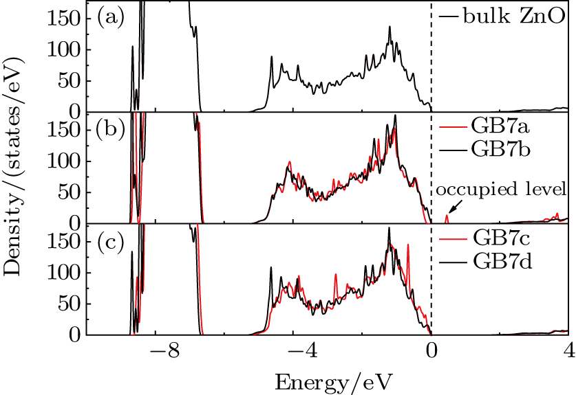
Detailed atomic configurations of the ZnO-Σ7() GB models are shown in Fig. 1. Two antiparallel GBs are included in one supercell. For each GB7a unit, there are four three-fold coordinated atoms, including two Zn (Zn04 and Zn08) atoms and two O (O04’ and O08’) atoms. In GB7b, two three-fold coordinated atoms exist in one unit, which contains one Zn (Zn01) atom and one O (O01’) atom. However, all of the atoms are four-fold coordinated in GB7c, similar to bulk ZnO. Different from the previous configurations, there are two five-fold coordinated atoms (one Zn (Zn01) atom and one O (O01’) atom) in each GB7d unit. So, the atoms in the twinned planes have different coordination states. In addition, expect GB7d, there are large open channels along the GB planes, which may favor the aggregation of impurities and native defects. Figure 2 shows the density of state (DOS) of bulk ZnO and four ZnO-Σ7() twin GBs. Compared with bulk ZnO, GB7a has an occupied level induced by O–O bonds above the VBM. Due to the large open channels, the O04’ atom is close to the O08’ atom and the distance is only 2.66 Å, which results in the formation of O–O bonds and an acceptor level above the VBM.[28] The other three twin GBs have similar DOSs to bulk ZnO.
Fig. 2. (color online) DOSs of bulk ZnO, GB7a, GB7b, GB7c and GB7d. The VBM of bulk ZnO is chosen to be zero in energy level.
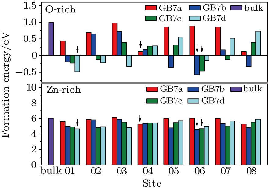
Generally, the GB planes can effectively release the strain caused by dopants. Due to the introduction of dopants, the open channel structures along the GB planes are broken, which weakens the lattice distortion and reduces the GB formation energies. From Fig. 3, we find that the AgZn in ZnO-Σ7() twin GBs has a lower formation energy than that in the bulk ZnO. Thus, AgZn in the GB planes should be more stable, comparing with that in bulk ZnO. Meanwhile, in consideration of the inversion symmetry in the twin GBs, several possible substitution sites are chosen for calculation, as shown in Fig. 1. The results are presented in Fig. 3. As expected, AgZn prefers to appear in the lattice distortion position and GBs can facilitate the formation of AgZn. The most stable positions are sites 04, 06, 06 and 01 in GB7a, GB7b, GB7c, and GB7d, respectively. In GB7a, due to the three-fold coordination, AgZn at site 04 only needs to break three Zn–O bonds, which results in a low formation energy. However, for GB7b, the most stable position of AgZn is the four-fold coordination site marked 06, instead of the three-fold coordination site marked 01. The relaxed configuration shows that AgZn at site 06 bonds with O01’. The distance between the two atoms is only 2.20 Å and the formation of a new Ag–O bond stabilizes the configuration. In addition, the introduction of AgZn at site 06 and site 01 in GB7c and GB7d, respectively, gains the lowest formation energy due to the strain relief.
Fig. 3. (color online) The formation energies of AgZn in ZnO-Σ7() GBs.
Table 1 lists the ionization energies of AgZn at the most stable position in ZnO-Σ7() twin GBs under O-rich (Zn-rich) conditions. In the bulk ZnO, the calculated ionization energy of AgZn is 0.37 eV above the VBM and the corresponding experimental value is about 0.4 eV.[16,39] Comparing to bulk ZnO, the ionization energy of AgZn in GB7a is reduce to 0.16 eV, which is the lowest value in the four GBs. The obtained results indicate that AgZn has the greatest potential to serve as a shallow acceptor in GB7a.
Table 1.
Table 1.
Table 1.
The formation energies and ionization energies of AgZn at the most stable position in ZnO-Σ7() GBs.
.
Site
Ef/eV (O-rich)
Ef/eV (Zn-rich)
ε(0/−1)/eV
Bulk ZnO
1.18
6.33
0.37
GB7a (at 04)
0.12
5.27
0.16
GB7b (at 06)
−0.58
4.57
1.09
GB7c (at 06)
−0.47
4.68
0.41
GB7d (at 01)
−0.49
4.66
1.06
Table 1.
The formation energies and ionization energies of AgZn at the most stable position in ZnO-Σ7() GBs.
.
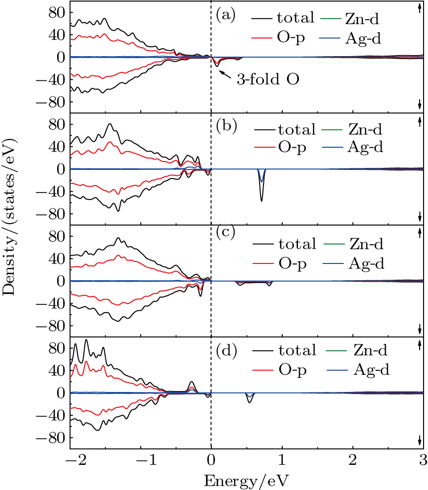
To explore the shallow acceptor behavior of AgZn, the DOS of AgZn at the most stable position in the ZnO-Σ7() twin GBs is shown in Fig. 4. For the four twin GBs, all the spin-up states are occupied and resonate with the valence band. The main asymmetry distribution is the discrete empty peak in the spin-down state near the VBM. As shown in Fig. 4(a), there are two empty spin-down peaks. One located at 0.08 eV is the antibonding state of O04’-2p and O08’-2p and the other located at 0.31 eV consists of the Ag-4d state. Due to the introduction of AgZn, the distance between the O04’ and O08’ atoms reduces to 2.47 Å, which induces the formation of an O–O bond in GB7a. The charge density of O–O antibonding in the spin-up state is shown in Fig. 5. It can be found that the antibonding state has an obvious p–p coupling character and points to each other. Meanwhile, the antibonding state of the p–p bond is partially occupied, which leads to a weak spin splitting. As a result, an empty energy level in the spin-down state appears just above the VBM, as shown in Fig. 6(b), which can serve as a shallow acceptor in GB7a. For GB7b and GB7d, the five-fold coordinated AgZn in GB7b and GB7d causes an empty spin-down localized state located at 0.71 eV and 0.62 eV, respectively, which mainly composes of Ag-4d orbital, as shown in Figs. 4(b) and 4(d). Similarly, for AgZn in GB7c, Figure 4(c) shows that two empty spin-down peaks at 0.41 eV and 0.82 eV are dominated by the Ag-4d orbital. The deep energy levels also mean high ionization energies in these three configurations.
Fig. 4. (color online) DOSs of AgZn at site 04 in GB7a, at site 06 in GB7b, at site 06 in GB7c and at site 01 in GB7d, respectively. The Fermi energy level is chosen to be zero.
Fig. 5. (color online) The isosurface (0.001 e/Å) of charge density of the O–O antibonding state in GB7a. Red, blue and silver spheres designate O, Zn and Ag atoms, respectively.
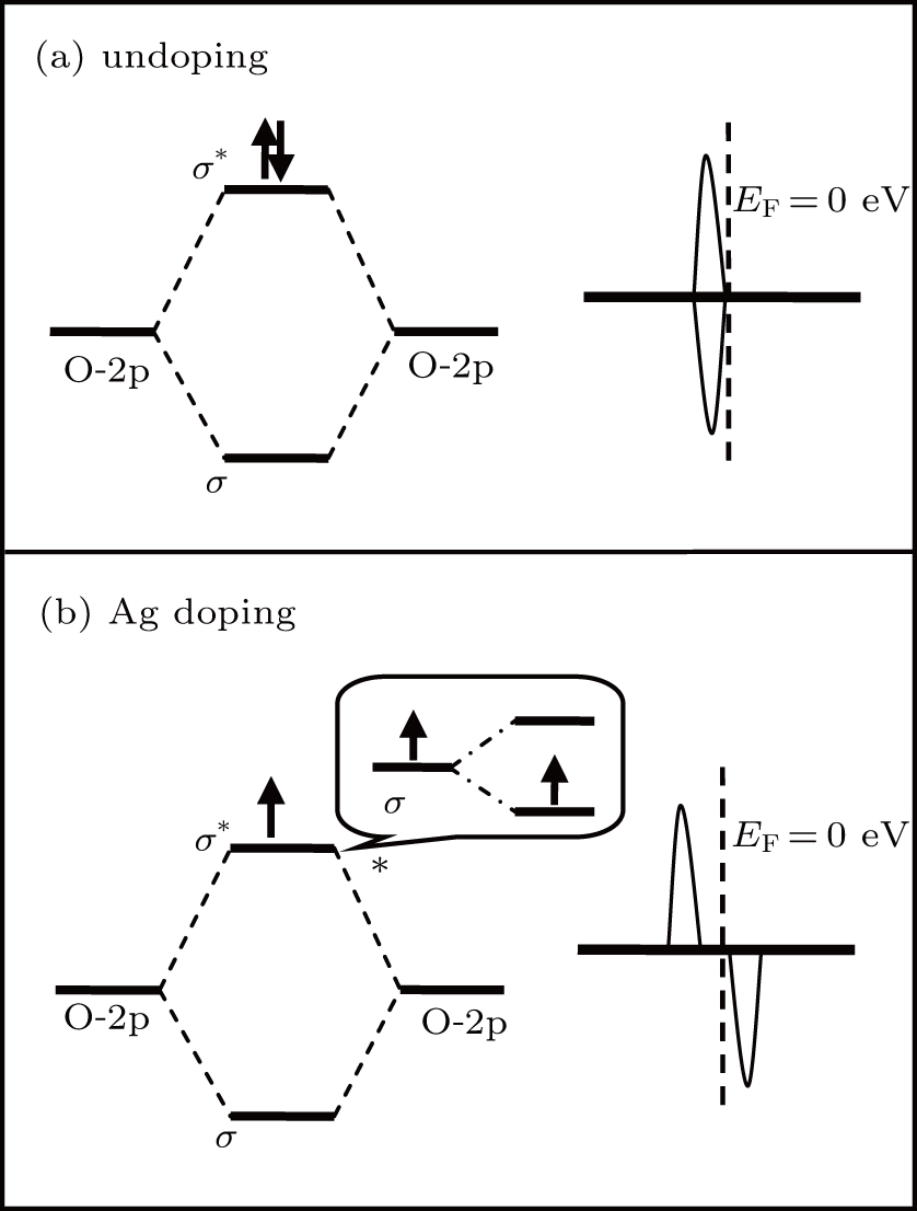
Fig. 6. Schematic representation of the energy level for the O–O bond in GB7a: (a) undoped, (b) Ag doping.
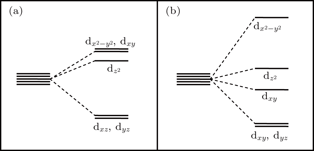
In order to further investigate the mechanism of the shallow acceptor character of Ag-doped GB7a, the energy level splitting in the four GBs with AgZn is discussed. As pointed out above, the p-d hybridization between Ag and its surrounding O atoms leads to deep energy levels, which may be explained by analyzing the split AgZn-d orbitals in ligand field.[40,41] In GB7c, four coordinated AgZn and its four neighbor O atoms arrange in the shape of a trigonal pyramidal, instead of a tetrahedron. According to the ligand field theory, there are two relatively high-energy Ag-4d orbitals in dx2−y2 and dxy, as shown in Fig. 7(a). This result corresponds to the two deep energy levels located at 0.41 eV and 0.82 eV shown in Fig. 4(c). In addition, in GB7b and GB7d, the five-fold coordinated configurations belong to the tetragonal pyramidal ligand field. In Fig. 7(b), a relatively high-energy Ag-4d orbital in dx2−y2 is observed, which corresponds to the empty spin-down localized state in Figs. 4(b) and 4(d) These results demonstrate that the acceptor levels induced by four and five coordinated AgZn are deep in ZnO.
Fig. 7. The split AgZn-4d orbitals in two ligand fields, including (a) trigonal pyramidal configuration and (b) tetragonal pyramidal configuration.
For GB7a, due to the incorporation of AgZn, the partially occupied antibonding state of the O–O bond undergoes a weak spin splitting, which eventually gives rise to a shallow acceptor state above the VBM. In fact, O–O bonds exist not only in GB7a, but also in other planar or linear defects. Therefore, if the acceptor impurities could bond with one O atom in the O–O bond, a shallow acceptor level is expected. In other words, the planar or linear defects, containing O–O bonds, may facilitate p-type doping in ZnO.
4. Conclusion
In summary, the electrical properties of the undoped and Ag-doped ZnO-Σ7() twin GBs were investigated using the GGA+U approach. It is found that the GBs can facilitate the formation of AgZn due to the strain release. The calculation shows that four and five coordinated AgZn can be found in GB7b, GB7c and Gb7d and induce high ionization energy. However, the ionization energy of AgZn in GB7a is very low. The main reason is attributed to the O–O bonds in GB7a. When AgZn bonds with one O atom in the O–O bond, weak spin splitting occurs in the antibonding state of the O–O bond, which induces a shallow empty acceptor energy level above the VBM. The O–O bond model also can be applied to the future design of p-type doping in ZnO.
Effect of O–O bonds on p-type conductivity in Ag-doped ZnO twin grain boundaries*
Project supported by the National Natural Science Foundation of China (Grant No. 11364009) and Natural Science Foundation of Guangxi Province, China (Grant No. 2014GXNSFFA118004).


