


Quantitative HRTEM and its application in the study of oxide materials
Cite this Article
Jia Chun-Lin, Mi Shao-Bo, Jin Lei. Quantitative HRTEM and its application in the study of oxide materials. Chinese Physics B, 2018, 27(5): 056803 
Permissions
Quantitative HRTEM and its application in the study of oxide materials
† Corresponding author. E-mail:
Abstract
On the basis of a state-of-the-art aberration-corrected transmission electron microscope, the spherical aberration coefficient CS of the objective lens can be tuned to either a positive or a negative value. The use of a negative value of CS combined with an overfocus setting of the objective lens leads to the development of the negative CS imaging (NCSI) technique. Images obtained using the NCSI technique show superior contrast and signal intensity at atomic column positions than the corresponding positive CS images, especially for weakly scattering oxygen columns that are in close proximity to strongly scattering cation columns in oxides. Based on the images obtained under the NCSI condition, quantification of the image contrast allows measurements of the atom positions with a precision of a few picometers and the local chemistry on atomic scale. In the present review, we discuss firstly the benefits of the NCSI technique in studies of oxide materials, and then show a procedure for quantitative analysis of the image based on the absolute value of contrast. In the last part, examples are given for the application of the quantitative high-resolution transmission electron microscopy (HRTEM) to the study of electric dipoles of oxide ferroelectrics and atomic-scale chemistry of interfaces.
Keyword:quantitative high-resolution transmission electron microscopy (HRTEM);negative CS imaging (NCSI);aberration-correction;functional oxides
1. Introduction
Oxide materials have become increasingly important for electronic applications. In particular, oxide thin films have been the most important material basis for various electronic devices such as non-volatile ferroelectric random-access memory (FRAM) and high density dynamic random access memory (DRAM).[1,2] Lattice defects including interfaces, dislocation and local chemical variation have attracted great attention of research since these defect areas show different electrical properties from the perfect lattice areas.[3–6] These unexpected properties can be considered for application in devices for novel functions.[7] Heterointerfaces and dislocations in oxide systems and domain walls in ferric materials are particularly interesting since these lattice defects can be engineered by the thin film technology[8,9] and their properties and corresponding structure feature can be tested and investigated by various techniques.
Transmission electron microscopy (TEM) has proven to be a powerful tool for materials research. In particular, in the recent decade, great progress in the techniques of high-resolution TEM (HRTEM) has been made by the successful introduction of the spherical aberration (CS) correctors.[10] Based on the aberration-corrected electron microscope, the point resolution of sub-Å has been achieved.[11] For crystalline materials, the aberration-corrected electron microscopy can be used for determining the position of atomic columns with a precision of a few picometers and the chemical occupancy in atomic columns with a precision of a few atomic percent. With quantitative evaluation of image contrast of a thin crystal, the number of atoms within the atomic columns parallel to the viewing direction has been determined. Up to now, it is possible to characterize the three-dimensional shape of nanoscale crystal with single atom precision.[12]
In comparison with TEM, other structure characterization techniques, such as x-ray and neutron scattering, which are reciprocal-space techniques, provide averaged real-space information from macroscopic areas of material samples. TEM can reveal the structural information from micro-scale to atomic scale. Therefore, TEM and HRTEM are desired techniques for studying the real structural feature at defect-affected areas of matter with sub-Å resolution.
In the present review, we focus our discussion on quantitative HRTEM based on negative CS imaging (NCSI) technique[13,14] and its applications in studying oxide materials.
2. NCSI technique and benefit to image contrast
where λ is the electron wavelength,

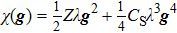
is a vector in the real space and t is the specimen thickness. The wave propagating through the objective lens suffers additional phase shift due to the lens aberrations, among which the spherical aberration coefficient CS and defocus value Z are two chief parameters. Using different CS-defocus combinations, we can tune the phase shift of the scattered wave by tuning the aberration function
, where

is the diffraction vector in the reciprocal space. The classical PCSI condition for optimum phase contrast is obtained by combining a positive value of CS with an underfocus, which results in a dark-atom contrast. The NCSI condition with a negative value of CS cooperating with an overfocus leads to a bright-atom contrast.[13]
if the objective lens adds a phase of

or

to the diffracted wave, resulting in image intensity recorded in the image plane
which is correct to the second order in

. Under the NCSI imaging condition, the sign of the linear term of Eq. (3 ) is positive and thus the linear and nonlinear terms are additive.[14] In contrast, for the PCSI condition, the sign of the linear term of Eq. (3 ) is negative and thus the linear and nonlinear terms are subtractive.
In this section, we introduce an imaging technique based on CS-corrected TEM, the NCSI technique,[13,14] which results in a high-contrast of image in comparison with the conventional positive CS imaging (PCSI) technique. In order to understand the contrast enhancement under NCSI conditions, an approximation for the object, i.e., weak phase object (WPO), has to be used.
In a very thin specimen, the phase of the propagating electron wave is modified by the object potential. At the exit plane, the wave function 

 |
On the basis of Eq. (
 |
 |
Clearly, the contrast modulation due to the projected potential 
Figure
 | Fig. 1. (color online) Simulated images of STO viewed along the [110] direction under (a) the NCSI condition with 

|
For obtaining reliable results from quantitative HRTEM, a key requirement is the good enough signal intensity of the images, which determines the precision for measurement of the positions and occupancy of the atomic columns in real structure. Figure
 | Fig. 2. (color online) Profiles of image intensity for atomic columns of SrO, Ti and O from the NCSI image shown in Fig. |
Based on the images of the STO crystal shown in Fig.
The dependence of the signal intensity on the atomic number accumulated in individual atomic column was also investigated under both NCSI and PCSI conditions. Along the [110] direction of STO, a unit cell period includes two oxygen atoms in the pure oxygen column, one Ti atom in the Ti column and one Sr atom plus one oxygen atom in the SrO column. Therefore, over a single unit cell period, the sum of atomic numbers in the fully occupied column is 16 (2×8), 22 and 46 (8 + 38) for the oxygen column, the Ti column and the SrO column, respectively. As shown in Fig.
 | Fig. 3. (color online) Image intensity as a function of the sum of atomic number in atomic columns along the [110] direction of STO for different sample thicknesses under the NCSI condition (solid symbols) and under the PCSI condition (open symbols). The different colors are for different thicknesses of atomic columns.[15] |
Based on the image simulations, we have demonstrated that the images obtained under the NCSI condition show great advantages with respect to image contrast, signal intensity for atomic columns, and the linear dependence of the intensity on the atomic number in atom columns. The special features of the negative CS images are the result of the combining enhancing of the phase contrast with amplitude contrast.[15,16] Therefore, the NCSI technique provides optimum HRTEM condition for direct atomic imaging of material structures, which is the basis for quantitative determination of atomic structures by aberration-corrected TEM.
3. Iterative procedure for quantitative HRTEM based on NCSI
Based on the above results and discussion, under the NCSI conditions, the positions of the image intensity maxima represent already quite well the actual positions of atomic columns. Likewise, for a thin specimen, the height of the intensity maxima is roughly proportional to the accumulated atomic charge number along an atomic column. However, it should be noted that in experiment, residual lens aberrations and small tilts of the specimen orientation away from the fully symmetric Laue orientation are unavoidable and thus affect the contrast of atomic-resolution images, i.e., the positions and image intensity maxima. This means that the images recorded in the microscope include not only the structure information, but also artifacts induced by the deviation from the ideal imaging conditions. In addition, a linear relationship between the observed peak intensity and the actual atomic column occupation is not guaranteed due to the nonlinear nature of electron diffraction. Therefore, in most cases, the data measured directly from an HRTEM image cannot simply be used as the real atomic feature for interpretation of various properties of materials. Comparison between the experimental image and the simulated one is the most accurate route for removing these artefacts and thus precisely determining the structure of materials at atomic scale.
In practice, an iterative procedure for image comparison is used, as schematically shown in Fig. 


 | Fig. 4. (color online) Schematic of an iterative procedure for quantitative comparison between experimental and simulated images for determining the true atomic structure of material.[12] |
An additional problem is the frequently observed systematic mismatch of the magnitude of the image contrast between simulation and experiment, which was proposed firstly by Hÿtch and Stobbs.[17] For solving this so-called Stobbs-factor problem, in image simulation, the other effective factors dampening image contrast also need to be taken into account, e.g., the modulation transfer function (MTF) of the used charge-coupled-device (CCD) camera[18] and additional image contrast spread function.[12,19] With considering all these effects, HRTEM images are simulated and compared with the experimental image in an iterative way so that the best match between the simulated and experimental images is obtained. Only in the case of the best fit between the experimental and the simulated images with respect to positions and the intensity values of the intensity peaks as well as the true value of the image contrast, one can conclude that the structure model underlying the simulation represents indeed the actual atomic structure.
An excellent example for quantitative HRTEM is the work on determination of three-dimensional shape of MgO nanoscale crystal with atomic resolution.[12] In the work, a complete quantification of experimental and simulated images was performed with an accurate calibration of the relationship between a given atom column and the resulting image intensity. Figure
 | Fig. 5. Comparison of true contrast between the experimental (a) and the best fitting simulated (b) images of MgO. i and j index the intensity maxima, which were quantified with respect to the absolute intensity and geometric position. (c) The difference image between the experimental (a) and the best fitting simulated (b) images. (d) The difference image with enhanced intensity by adding the value of the mean intensity of the normalized simulated image. Note that all of the images are displayed with the same intensity scale.[12] |
Figure
 | Fig. 6. (color online) (a) Comparison of the data derived directly from the experimental image shown in Fig. |
In the following, examples are presented for the application of the quantitative HRTEM based on the NCSI technique to characterization of atomic structure and properties of oxides.
4. Atomic-scale study of electric dipoles across domain walls
The physical properties and structures of domain walls in ferroelectrics and multiferroics have been studied theoretically and experimentally.[20–27] It was found that the domain walls possess different properties depending on the atomic details of the walls. The novel properties at domain walls stimulate great interest in experimentally exploring the structure of domain walls at atomic scale.
4.1. Domain walls in ferroelectric PbZr0.2Ti0.8O3 films
Figure 

 | Fig. 7. (color online) (a) The cubic structure of paraelectric PZT at high temperature. (b) The tetragonal structure of ferroelectric PZT. (c) Six possible domains and relative domain walls. |
Figure 

 | Fig. 8. (color online) Atomic-scale image of a STO/PZT/STO thin-film heterostructure, recorded along the [

|
We are particularly interested in the part of domain wall on the left side of Fig.
 | Fig. 9. (color online) (a) Image of an LDW segment. Arrows denote the geometric central plane of the domain wall, which is referred to as the origin for quantitative analysis of the dipole distortion across the domain wall area. (b) The displacements of the Zr/Ti atoms (δZr/Ti) and the O atoms (δO) across the LDW. Positive values denote upward shifts and negative values downward shifts. (c) The spontaneous polarization 
|
In Fig. 


 | Fig. 10. (color online) (a) Atomic-resolution image of the 180° domain structure in a PZT film close to the interface to the STO substrate, recorded along the [110] direction. The interface is marked by a horizontal dashed line. The domain wall is indicated by a yellow dotted line and the polarization is denoted by arrows. In the center of the lower half of the image, a dotted blue line surrounds an area, where in the center, the polarization direction makes an angle of 90° with the two large domains. The inset on the right-hand side shows a calculated image demonstrating the excellent match to the experimental image. (b) Map of the displacement vectors for the Zr/Ti atoms (arrows) from the center of the projected oxygen octahedra. The arrows represent electric dipole moment of unit cell. Note that the continuous rotation of the dipole directions from “down” (right) to “up” (left) closes the electric flux of the two 180° domains. (c) Magnification of upper part of (a) and (b), showing details of the domain wall facets where polarization charges depolarize the nearby unit cells and reduce the off-center displacements of the atoms in these unit cells.[23] |
Figure
In the image of Fig.
The off-center displacements of the atoms were quantified by the iterative procedure based on the image in Fig. 
We note also facets in the upper part 180° domain wall, which is reproduced at larger magnification in Fig.
4.2. Domain walls in multiferroic BiFeO3 crystal
BiFeO3 (BFO) is a room-temperature multiferroic that simultaneously displays ferroelectric and antiferromagnetic properties. BFO has a rhombohedral structure with R3c space group. It can be derived from the perovskite structure by applying a tensile distortion along the direction of a body diagonal 

 | Fig. 11. (color online) (a) Perovskite unit cell of pseudocubic structure of BFO. (b) Projected structure along the [110] direction of the pseudocubic structure.[30] |
Figure 

 | Fig. 12. (color online) (a) Atomic resolution image of domains and domain walls in BFO crystal recorded parallel to the 


|
The off-center displacements of the Fe atoms and the rotation angles of the O octahedra were studied quantitatively for DW3 and the adjoining domains D2 and D3. In measurement of the displacements of the Fe atoms and the rotation angles of the oxygen octahedra, the effects of residual lens aberrations and unavoidable small tilt of the crystal have been removed in the iterative procedure for quantitative comparison between experimental and simulated images. Figure
 | Fig. 13. (color online) (a) Map of the off-center displacements of Fe atom positions in domains D2 (green arrows) and D3 (blue arrows) and in the domain wall area DW3 (red arrows in blue area) projected onto the {110} plane. (b) Map of the magnitude of the oxygen octahedron rotation angle, α, projected into the {110} plane. The area of DW3 is indicated by a white dotted line. A color scale denotes the tilting angles of oxygen octahedra and the magnitude of magnetization.[30] |
Recent investigation of dipole configurations in proper ferroelectrics (BaTiO3) by theoretical calculations showed that nontrivial configurations of dipoles could be stabilized by a new mechanism of topological protection, the finite-temperature fluctuations of local dipoles.[32] It was pointed that in order to classify topological defects, one need to explore the topology of full manifold of internal states, that would involve all values of accessible dipoles, in contrast to the local dipoles that are limited by the symmetry-allowed lattice directions. The important results of the work are the sufficiently high thermal entropy, which allows the local dipoles to significantly deviate from orientations defined by the symmetry allowance. Our experimental observations show indeed the nontrivial configuration of the local dipoles that deviate significantly from the [111] direction in the BFO crystal.
Figure
5. The structure and chemistry across a single-unit-cell layer of LaAlO3 embedded in SrTiO3
Novel functional properties of the interface between insulating LaAlO3 (LAO) and STO have been measured, including metallic conductivity, superconductivity and magnetism. These physical phenomena, which are not intrinsic to the bulk material, can be related to the local atomic rearrangements at the interface, the special feature of the oxide structure, and the strong correlation of electrons to the ionic lattices. For a comprehensive understanding of the origin of these novel properties, subtle details of the atomic structure at the interface area must be taken into account. A simultaneously quantitative determination of the structural and the chemical details at an identical specimen area has become great challenge of transmission electron microscopy. By means of quantitative HRTEM, which is described in Section
Figure
 | Fig. 14. (color online) (a) Atomic-resolution image of the nominally single unit cell layer of LAO embedded in STO, which was recorded along the [110] direction of STO under the NCSI condition. (b) The averaged image over the image area of (a). (c) Simulated image with the best match to the experimental image. The arrow denotes the nominally single LaO plane.[19] |
The final data are displayed in Fig.
 | Fig. 15. (color online) (a) The shifts of the AO-type columns (SrO and LaO), and of the oxygen columns across the single unit cell layer. (b) Chemical occupancy. The position of the nominal LaO atomic plane is marked by a vertical thick line.[19] |
6. NCSI with the CS/CC-corrected TEM
In a CS and CC (chromatic aberration) corrected electron microscope, such as Jülich PICO 50-300 microscope equipped with an advanced version of C-COR corrector (C-COR+, CEOS GmbH), the two major resolution limitations of the previous instrument generations due to partial spatial and partial temporal coherence are significantly reduced. The C-COR+ corrector allows unwanted coherent axial aberrations of the imaging system to be effectively reduced up to the fourth order, thereby obtaining optimum phase-contrast transfer up to the information limit by adjusting also the fifth-order spherical aberration (C5).[11]
Under optimum contrast transfer for the NCSI conditions, the instrumental resolution as defined by the information limit is measured using a diffractogram of gold nanoparticles supported by amorphous carbon to be below 50 pm for both 200 and 300 kV TEM and better than 80 pm at 80 kV. However, such measurement has been shown to depend on a number of sample related influences as well as on dynamic and non-linear diffraction effects which may result in an overestimation of the resolving power. Consequently, the concept of object resolution has to be introduced in practical case for the direct perception of resolution by considering the sample-related parameters.
In order to demonstrate the resolving power of the CS/CC-corrected PICO microscope, a b-axis oriented yttrium-aluminum perovskite (YAP) was selected.[11] At room temperature, YAP has the orthorhombic structure (space group Pnma) with lattice parameters a = 0.5330 nm, b = 0.7375 nm and c = 0.5180 nm, as schematically shown in Fig.
 | Fig. 16. (color online) (a) Schematic view of 2×2×2 orthorhombic unit cells along the crystallographic b zone axis of YAP. The 57 pm Y–Y-atom pair separation is indicated along two directions by the bold lines. Corners of squares give position of O atoms and centers denote positions of Al overlapping with O atoms. (b) Experimental image of YAlO3:Ce in the [010] projection. Arrows denote examples of Y–Y atom pairs with pair separations given.[11] |
It should be emphasized that the resolution improvement by the CS/CC correction is of critical importance particularly for the low acceleration voltage. This allows direct visualization of atomic structures in many beam sensitive materials, such as 2D materials (e.g., graphene, metal dichalcogenides, etc) and related structures,[34] although such materials are not the focus of the present review.
7. Summary
We have demonstrated with several examples that structural details, such as the atom positions and chemical occupancy in atomic columns that are parallel to the electron beam, can be obtained from a single HRTEM image. By quantitative comparison of image simulations with the experimental images recorded under the NCSI condition, the atom displacements can be measured with a precision of a few picometers. For ferroelectric materials, based on the precisely determined off-center displacements, the electric dipole of unit cell can be calculated and thus the local polarization can be investigated across the domain walls and lattice defect areas. For some magnetic oxides, local magnetization can also be studied taking the simple relation to the rotation angle of the oxygen octahedra. By quantitative analysis of the image contrast, the intermixing of cations in atomic columns and oxygen deficiency at an interface can be determined. In addition to the above-described examples, another excellent application of the quantitative HRTEM is to determine the three-dimensional shape of a MgO nanocrystal with atomic resolution from a single image. The successful application of the quantitative HRTEM to solving structural problems has played an important role in understanding the relations between structure and properties of materials and is expected to make more progress in the future materials research. On the other hand, based on TEM, other analytical techniques are available, such as electron diffraction, electron holography, scanning TEM imaging and various spectroscopic techniques. Combination of all these techniques provides the optimum capability for insight into the atomic details responsible for the various properties of materials.
Reference
| [1] | |
| [2] | |
| [3] | |
| [4] | |
| [5] | |
| [6] | |
| [7] | |
| [8] | |
| [9] | |
| [10] | |
| [11] | |
| [12] | |
| [13] | |
| [14] | |
| [15] | |
| [16] | |
| [17] | |
| [18] | |
| [19] | |
| [20] | |
| [21] | |
| [22] | |
| [23] | |
| [24] | |
| [25] | |
| [26] | |
| [27] | |
| [28] | |
| [29] | |
| [30] | |
| [31] | |
| [32] | |
| [33] | |
| [34] |