Distinction between critical current effects and intrinsic anomalies in the point-contact Andreev reflection spectra of unconventional superconductors
He Ge1, 2, †, ‡, Wei Zhong-Xu1, 2, †, Brisbois Jérémy3, †, Jia Yan-Li1, 2, Huang Yu-Long1, 2, Zhou Hua-Xue1, 2, Ni Shun-Li1, 2, Silhanek Alejandro V3, Shan Lei1, 2, 4, Zhu Bei-Yi1, Yuan Jie1, Dong Xiao-Li1, 2, 4, Zhou Fang1, 2, 4, Zhao Zhong-Xian1, 2, 4, Jin Kui1, 2, 4
Beijing National Laboratory for Condensed Matter Physics, Institute of Physics, Chinese Academy of Sciences, Beijing 100190, China
School of Physical Sciences, University of Chinese Academy of Sciences, Beijing 100049, China
Experimental Physics of Nanostructured Materials, Q-MAT, CESAM, Université de Liège, B-4000 Sart Tilman, Belgium
Collaborative Innovation Center of Quantum Matter, Beijing 100190, China


† Corresponding author. E-mail: gehe@iphy.ac.cn

Abstract

In this work, we discuss the origin of several anomalies present in the point-contact Andreev reflection spectra of (Li1−xFex)OHFeSe, LiTi2O4, and La2−xCexCuO4. While these features are similar to those stemming from intrinsic superconducting properties, such as Andreev reflection, electron-boson coupling, multigap superconductivity, d-wave and p-wave pairing symmetry, they cannot be accounted for by the modified Blonder–Tinkham–Klapwijk (BTK) model, but require to consider critical current effects arising from the junction geometry. Our results point to the importance of tracking the evolution of the dips and peaks in the differential conductance as a function of the bias voltage, in order to correctly deduce the properties of the superconducting state.

1. Introduction

Point-contact spectroscopy (PCS) has proved to be a simple yet powerful tool for investigating the properties of metallic and superconducting materials.[1] This technique relies on the formation of a point-contact between two metals, or a metal and a superconductor, allowing for a current I to flow through the resulting junction when a bias voltage V is applied. Typical experiments consist in measuring differential conductance spectra, whose characteristic features can be associated with intrinsic material properties. On the one hand, electrons might pass from the tip to the sample by tunneling through the potential barrier at the interface. In this situation, is proportional to the density of states in the sample and gives some insight into the electronic properties of the material. On the other hand, in superconducting samples, electrons with an energy smaller than the superconducting gap Δ can tunnel through the interface by pairing up with another electron to form a Cooper pair. This process, known as Andreev reflection, leads to the reflection of a hole with opposite spin than the incident electron, in order to satisfy spin and charge conservation.[2] Point-contact spectroscopy in the Andreev reflection (PCAR) regime has been widely employed to study conventional superconductors, as is strongly related to several critical properties such as Δ, pairing symmetry or electron-boson coupling, to name a few.[1,3]

In comparison to conventional superconductors, unconventional superconductors host a rich diversity of phenomena, including pseudogap,[4] d-wave/p-wave pairing symmetry[5,6] or multi-band superconductivity,[7,8] that influence the PCAR spectra. For instance, if tunneling occurs along the nodal direction, a zero bias conductance peak (ZBCP) is detected around V = 0. This effect, arising from the Andreev reflection between positive and negative phase in a k-dependent nodal gap,[9] was evidenced in La2−xCexCuO4 and YBa2Cu3O7−δ.[10,11] Another example is the appearance of dips and ZBCP in the differential conductance spectra, indicating the existence of p-wave superconductivity.[12,13] This is due to the existence of non-trivial topological edge modes. The existence of multiple energy gaps arising from multi-band superconductivity also leaves a clear imprint in the spectra, when the coupling between the gaps is weak. This was namely observed in MgB2[14,15] and in iron-based superconductors (FeSe,[16] (Li1−xFex)OHFeSe,[17] LaFeAsO0.9F0.1,[18,19]) as evidenced by the observation of multiple coherence peaks.

Although the anomalies observed in the PCAR spectra might originate from the intrinsic properties of the unconventional superconductors under study, other less exciting phenomena related to the configuration of the junction between the tip and the sample surface should be seriously considered. Indeed, similar anomalies were widely observed both in conventional and unconventional superconductors and were attributed to diverse causes such as the superconducting proximity effect, the formation of an intergrain Josephson junction at the tip apex or heating in the point-contact, leading to a local decrease in the critical current of the superconductor.[20,21] Therefore, caution has to be exerted when interpreting the experimental data. In particular, phenomena inducing intrinsic properties of the sample and those related to the geometry might give similar features in the spectra. This could lead to erroneous conclusions on the nature of superconductivity in unconventional superconductors if the Blonder–Tinkham–Klapwijk (BTK) model,[22,23] usually employed to describe the spectra, is not amended to account for the additional effects.

In this work, we aim at clarifying the interpretation of experimental PCAR spectra, by making a clear distinction between anomalies arising from the intrinsic properties of unconventional superconductors and those coming from the junction geometry. In particular, we address the situation where the reduction of the superconducting critical current plays a crucial role in the interpretation of the data. This is the case (i) when heating occurs in the point-contact and (ii) when the tip is in series with an intergrain Josephson junction. After that we briefly review the proximity effects which will introduce similar anomalies. Under these circumstances, the results from the BTK model need to be complemented by additional contributions to account for the features in the spectra. With this in hand, we are ready to confront the theoretical description to some experimental examples of PCAR on unconventional superconductors, where it is of paramount importance to go beyond the BTK model to properly understand the superconducting properties of the sample. The experiments shed light on possible misinterpretation of the spectra, arising from the confusion between critical current effects and i) Andreev reflection, ii) multiband superconductivity, iii) p-wave superconductivity, and iv) d-wave superconductivity.

2. Modelling the critical current effects
2.1. BTK model

An ideal point-contact junction essentially consists in a metal in the non-superconducting state (N) brought in contact with a superconductor (S), separated by a thin insulating barrier (I). A simplified model, the so-called BTK model,[23] has been introduced by Blonder, Tinkham, and Klapwijk to describe PCAR in such N/I/S junctions. Assuming a unidimensional junction at zero temperature, aligned with the x axis, the repulsive insulating barrier at the interface is represented by the potential energy . The transparency of the barrier is proportional to where the parameter , with the Fermi velocity.

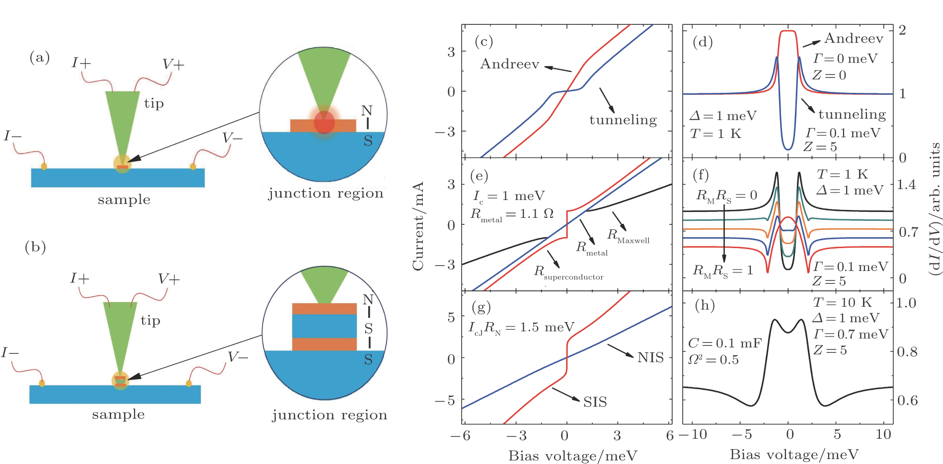
Under these assumptions, the current INIS across the junction can be calculated analytically, by considering the probability of occurrence of different processes that an electron coming from the N side may undergo at the interface. In the BTK model, these include Andreev reflection (with a probability A), ordinary specular reflection (B), and transmission as an electron-like (C) or hole-like (D) quasiparticle. As a result, the current INIS can be written as where V is the junction bias voltage, E is the energy, is the Fermi distribution function and Ia is a constant depending on the junction constitution and geometry. The typical dependence of INIS on V is represented in Fig. 1(c) for two values of Z corresponding to extreme regimes. In all cases, for , the dominant conduction mechanism is the transmission of electrons through the interface as quasiparticles. For , the regime of conduction is strongly dependent on the value of Z. On the one hand, if Z is low, meaning that the tip is close to the sample surface, Andreev reflection dominates, as shown by the red line in Fig. 1(c). On the other hand, if the insulating layer is thick, i.e., for high Z values, the conduction is essentially dominated by tunneling, as illustrated by the blue line in Fig. 1(c). Usually, the results of PCS experiments are represented in terms of the normalized differential through its value in the normal state. Figure 1(d) shows the curves corresponding to the two regimes illustrated in panel (c). The Andreev regime is characterized by an enhancement of the conductance at low V, where its value is doubled compared to the normal state. On the contrary, the hallmark of the tunneling regime is a dip at zero bias voltage.

Fig. 1. (color online) Response of a point-contact when critical current effects are accounted for. (a) and (b) Schematics of the typical assembly for point-contact spectroscopy measurements, where a tip is brought into contact with the sample. The current I (I+ and I−leads) is measured as a function of the bias voltage V (V+ and V−leads). The enlargement of the contact region shows the simplified structure described in the theoretical model: (a) an N/I/S junction with heating and (b) an N/I/S junction in series with a Josephson junction (S/I/S). N, I, and S stand respectively for normal metal, insulator and superconductor. (c) Typical I(V) dependence of the N/I/S junction calculated with the BTK model in two extremes regimes: Andreev reflection (red) and tunneling (blue). (d) Differential conductance spectra corresponding to the curves in panel (c). Here Γ represents the decay of finite quasi-particle lifetime by inelastic scattering. (e) Typical I(V) dependence of the Maxwell resistance RM (black) considering the contributions of the metallic tip and the superconducting sample (red). (f) Differential conductance spectra for several ratios. (g) Contributions of the N/I/S (blue) and S/I/S (red) junctions to the total resistance of the junction represented in panel (b). (h) Differential conductance spectra corresponding to the curves in panel (g).

As a final remark, note that the BTK model is valid only under the assumption that heating and proximity effects are negligible in the point-contact region. In practice, satisfying these conditions implies that the characteristic size a of the contact should be smaller than the electron mean free path l and the coherence length ξ, respectively.[8]

2.2. N/I/S junction in the intermediate regime

Up to now, we considered point-contacts with a small characteristic radius , where l is the inelastic mean free path. In this situation, the electrons are in the ballistic regime and cross the point-contact without scattering, thus without dissipation. The resistance of the contact (in the normal state, ) is then given by the Sharvin resistance[24] where ρ is the resistivity, proportional to . Therefore RS essentially depends on the geometry of the point-contact. In the general case of a contact between two different materials, in the free-electron approximation and assuming a spherical Fermi surface for both the metal and superconductor, RS can be written as[25] where and Parameters kF and vF correspond the Fermi momentum and Fermi velocity. The subscript indices m and s relate to the metal and the superconductor, respectively.

On the contrary, in the thermal regime where , the resistance is mostly determined by the resistivity of the materials as given by the Maxwell resistance Since electrons are scattered in the point-contact, Joule heating occurs and the temperature Teff at the center of the contact is higher than the environment temperature T and can be approximated by[26] where L is the Lorenz number. In metals, and even more so in superconductors, ρ increases as T raises. Compared to the isothermal situation, local heating will therefore result in a steeper increase of ρ as V is increased.

In general, in the situation depicted in Fig. 1(a), the point-contact lies in an intermediate regime where the total resistance R is made of the combined contributions of RS and RM[27] where the function is on the order of 1 and varies slowly with l/a. Since , while , the resistance of small contacts is dominated by RS, while RM becomes preponderant for large contacts.

The features of RS have been described previously by the BTK model. The I(V) characteristics of RM can be plotted using Eq. (5) as shown in Fig. 1(e). The red curve gives an example of a typical I(V) curve for a superconductor, while the metal is represented in blue. If a current is applied to measure the I(V) curve of the junction, the total voltage of the junction from Maxwell resistance is the sum of Vmetal and Vsuperconductor. At a current higher than the critical current (Ic) of the superconductor, the superconductor turns into a normal metal. Thus, the I(V) curve obeys the Ohmʼs law. However, when the current is close to Ic, the resistance of the superconductor decreases rapidly and the total voltage decreases, leading to the observation of a prominent nonlinear feature. Until a current lower than Ic, the I(V) characteristics are determined by the metal. Most of time, due to the heating effect, the I(V) curve might deviate from the linear behavior in this regime, depending on the effective temperature governed by Eq. (6). Tuning the value of , we obtain a normalized spectra as represented in Fig. 1(f). Due to the existence of Ic in the superconductor, two dips can be observed in the spectra in the intermediate regime. With the decrease of , the magnitude of the dip decreases gradually.

2.3. Critical current effects in N/I/S and S/I/S (S/N/S) junctions in series

In polycrystalline superconductors, where the intergrain weak-coupling effect plays an important role, the BTK model does no longer provide a satisfying description of the junction. Indeed, in this situation, the junction between the tip and the sample surface can in general be represented by the point-contact (N/I/S) described previously, associated in series with a Josephson junction (S/I/S), accounting for the connection between the tip and the superconducting grains. This situation is depicted in Fig. 1(b).

The total voltage V across the junction is then the sum of two contributions: the point-contact voltage VNIS, described by the BTK model, and the Josephson junction voltage VSIS. In the presence of thermal noise and with the assumption that the associated capacitance C is small, the contribution of VSIS can be calculated by the resistively shunted junction (RSJ) model,[20,28] and is written as where I0 and I1 are the modified Bessel functions, RN is the normal state resistance, IcJ is the maximum Josephson current, , in which Tn is the effective noise temperature, and .

The I(V) curve corresponding to the typical response of a Josephson junction is shown in red in Fig. 1(g). In general, at , only Cooper pairs are able to pass through the junction, and V remains small. However, at , the Cooper channel gradually vanishes, whereas the Josephson junction I(V) turns to the quasiparticle branch with a certain normal resistance.

The features of the spectra resulting from the association of the NIS junction and SIS junction depend strongly on their normal-state resistances RNIS and RSIS, respectively. We can calculate the I(V) characteristic and the differential conductance by using the following relations: , . When current is lower than IcJ, VSIS is close to 0, and VNIS dominates the total voltage. However, with the increase of current, a remark enhancement of VSIS happens at IcJ, which leads to two dips in the curve as seen in Fig. 1(h).

In some point-contacts, the tip is not sharp enough, and Andreev reflection effect becomes weaker than a fine junction. In this case, SIS junction dominates the spectrum, and a ZBCP can be observed, which is higher than 2[20,29] (the maximum value expected from the conventional Andreev reflection). It is known that ZBCP is not expected for an ideal RSJ model except for a point of divergence at zero point. However, when a small normal RNIS connect in series with RSIS, at , I(V) curve has a large slope but not a vertical line, where the ZBCP can be observed. It is expected to observe two coherence peaks and ZBCP at the same time in an appropriate situation.

Finally, if the insulating layer in the SIS is substituted by a normal metal, i.e., SNS, multiple Andreev reflection may happen at the interface between the superconductor and the metal, which can also induce an enhanced ZBCP higher than 2.

2.4. Proximity effects

Proximity effects occurring at the interface between a metal and a superconductor might give rise to additional features in the conductance spectra.[30] Indeed, due to the diffusion of Cooper pairs from the superconductor to the metal, a weak superconducting layer is formed at the superconductor/metal interface, with a superconducting gap smaller than the bulk value. Therefore, Andreev reflection in the proximity effect layer occurs for voltages lower than the bulk value. However, the bias voltage still needs to be large enough to overcome the bulk gap, so a dip in the conductance spectrum appears between those values. The proximity effect can be accounted for by introducing two gap values in the model, giving rise to sharp dips between the voltages corresponding to the gap energies. This effect is more prominent in the case of a clean contact with a low Z.

3. Results and discussion
3.1. Experimental details

The point-contact junctions between the samples and the probe are established using home-made Pt/Ir tips or a small drop of Ag paste. The assembly is installed in a Quantum Design PPMS system to achieve temperatures as low as 1.8 K, and high magnetic fields, up to 15 T. Sample stage motion is allowed on the x-axis and z-axis, in the range of 3 mm and 2.5 mm respectively. The differential conductance , is measured as a function of the bias voltage V by a standard lock-in technique. The methods of growing the La2−xCexCuO4[31] films, LiTi2O4[32] films, (Li1−xFex)OHFeSe crystals,[33] and films[34] can be found elsewhere.

3.2. Distinction between critical current effects and Andreev reflection

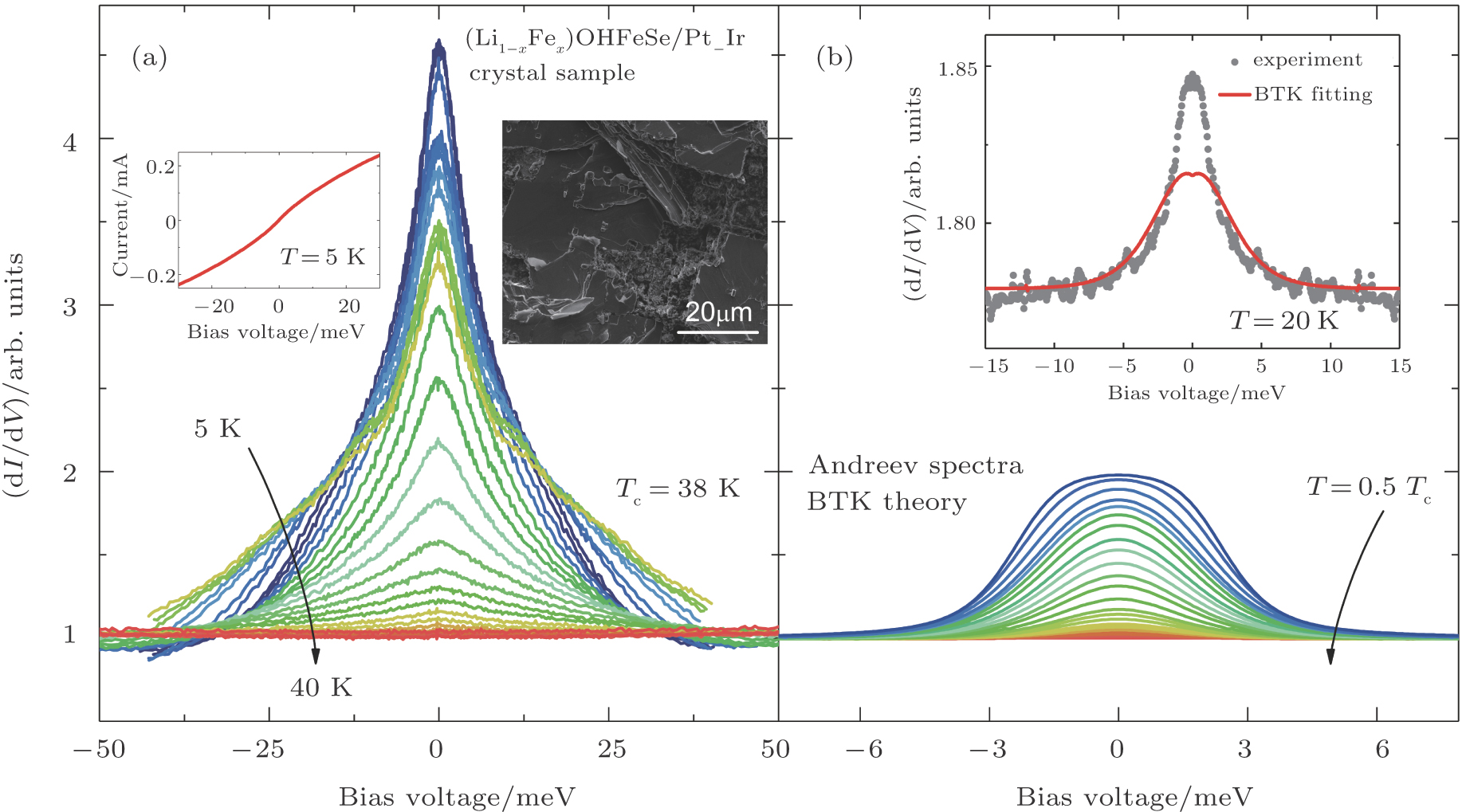
The experimental PCAR spectra obtained on a point-contact between an (Li1−xFex)OHFeSe sample and a PtIr tip are shown in Fig. 2(a), for temperatures between 5 K and 40 K. The inset represents corresponding I(V) curve at T = 5 K which is obviously nonlinear. The critical temperature of the sample is . A marked peak with an amplitude over 4 is present in the signal at low temperature. Its strength decreases as T increases and it vanishes around . At first sight, this feature seems related to the Andreev reflection observed for superconducting samples. However, a careful comparison with the BTK theory, represented in Fig. 2(b) for temperatures between and Tc, shows that Andreev reflection alone cannot account for the observed experimental spectra, as the shape and amplitude of the peak is significantly different. The fitting of the experimental spectrum at T = 20 K, represented in the inset of Fig. 2(b), clearly illustrates this point. As a consequence, if the BTK model is used to fit this data, incorrect information will be obtained on the superconducting properties, such as the superconducting gap Δ.

Fig. 2. (color online) Distinction between critical current effects and Andreev reflection. (a) PCAR spectra on an (Li1−xFex)OHFeSe sample with for temperatures between 5 K and 40 K. The inset shows the corresponding I(V) dependence at T = 5 K and the picture of surface taken by the scanning electron microscope. (b) Andreev reflection spectra obtained by calculations within the framework of the BTK model for temperatures between and Tc. The inset shows the clear discrepancy between the experimental curve at T = 20 K (dots) and the result of fitting with the BTK model (red line).

The differences between the experimental spectra and the BTK model can be attributed to critical current effects, arising from the formation of an S/I/S(S/N/S) junction at the apex of the tip or the thermal effect. Indeed, as explained previously, the response of such a junction might lead to a large peak at zero bias, with amplitude significantly larger than 2. In view of the picture taken by scanning electron microscope showing easily broken surface [See the inset in Fig. 2(a)], we prefer the case of weak-links between superconducting grains. The peak amplitude observed in the data can therefore be decomposed in two contributions coming from the Andreev reflection, with an amplitude close to 2, and the Josephson junction accounting for the rest. Moreover, the peak is sharper than for Andreev reflection, in agreement with the N/I/S + S/I/S(S/N/S) model we exposed above.

These spectra are usually observed in iron-based superconductors,[3] such as the sample we studied here, as their surface is often fragile. As a consequence, in the process of forming a point-contact between the tip and the sample, the surface frequently suffers degradation. The resulting debris or defects lead to the formation of an S/I/S(S/N/S) junction between the tip apex and the sample. Another possible explanation for the formation of these junctions involves the bad crystallinity of some samples, such as polycrystalline systems, where the intergrain coupling plays a significant role. A more compelling evidence would require nanoscopic imagin of the tip-sample interface which is not straighforward even with the technology available today.

3.3. Distinction between critical current effects and multiband or p-wave superconductivity

Various unconventional superconductors were found to exhibit a multiband behavior.[14,3537] For instance, in iron-based superconductors, Angle-Resolved Photoemission Spectroscopy (ARPES) measurements widely show a signature of multiband superconductivity, with a hole pocket in the Γ points and an electron pocket in the M point.[36,38] In these systems, PCAR spectroscopy is a tool of choice to extract information on the band coupling. In many compounds, such as FeSe[16] and (Li1−xFex)OHFeSe,[17] the spectra point to the existence of two superconducting gaps. However, caution has to be exerted when interpreting spectra, as the dips characteristic of multiband superconductivity look very similar to those induced by critical current effects.

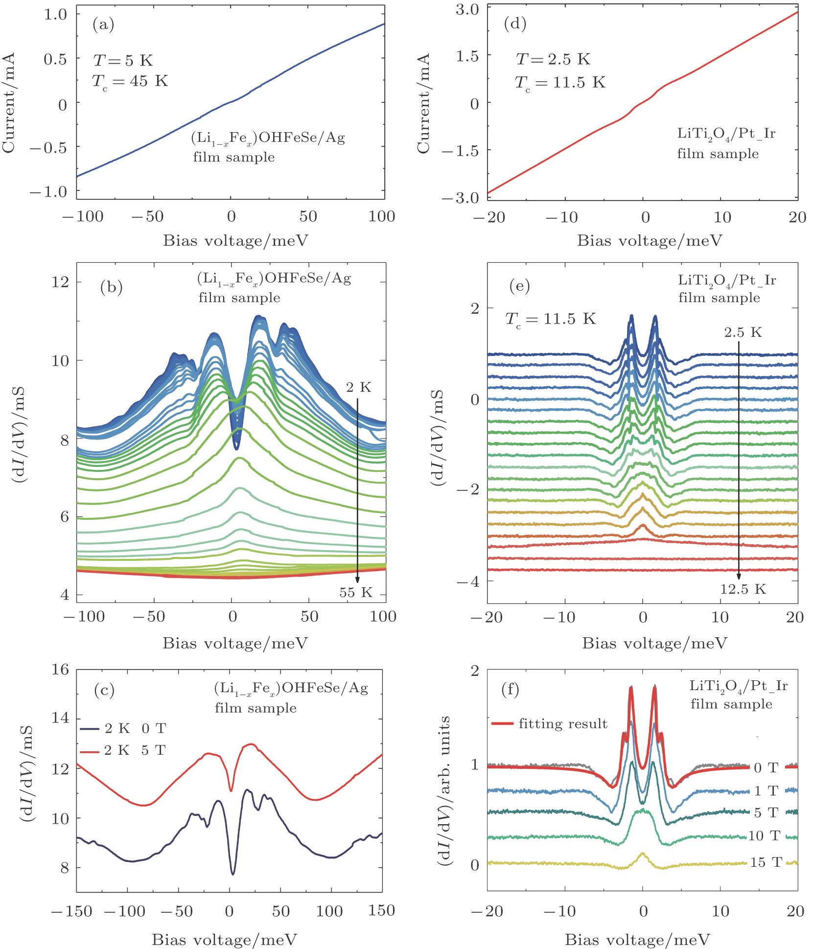
Figure 3(b) shows the experimental spectra for an (Li1−xFex)OHFeSe film with a critical temperature . Measurements are taken at temperatures ranging from 2 K to 55 K. At first sight, the dip structure might suggest the existence of multiband superconductivity. However, a more careful look shows that this explanation is incorrect and that the features in the spectra are actually explained by critical current effects. First, the energy scale associated with the dips is as high as 40 meV, while the features disappear at . These values give a coupling constant , much larger than the BCS value of 3.53, and are thus incompatible with the hypothesis of a BCS superconducting gap. This is further supported by the magnetic field dependence of the spectra, illustrated in Fig. 3(c) at 2 K for T (blue line) and T (red line), showing that the dips disappear at fields below 5 T. However, it is well known that in (Li1−xFex)OHFeSe samples, the upper critical field is typically larger than 100 T.[39] The suppression of the dips at and is due to the fact that the tip locally depletes superconductivity, possibly forming S/I/S junctions in the process. On the other hand, the I(V) curve at T = 5 K in Fig. 3(a) shows many bends, which also indicate the spectra contain some intrinsic information.

Fig. 3. (color online) Distinction between critical current effects and multiband or p-wave superconductivity. (a) The I(V) curve of (Li1−xFex)OHFeSe film at T = 2 K with a critical temperature . (b) spectra of (Li1−xFex)OHFeSe film, for T between 2 K and 55 K. (c) spectra of (Li1−xFex)OHFeSe at 2 K for a magnetic field T (blue line) and T (red line). (d) The I(V) dependence of LiTi2O4 film at T = 2.5 K with a critical temperature . (e) spectra of LiTi2O4 film, for T between 2.5 K and 12.5 K. (f) spectra of LiTi2O4 for magnetic fields between 0 T (blue line) and 15 T (red line) at 2.5 K.

For p-wave superconductors, PCAR spectra show double dips and ZBCP, resulting from the existence of non-trivial edge modes in unconventional topological superconductors.[13] These features have been observed in CuxBi2Se3,[12] Cd3As2,[40] and TaAs.[41] We performed PCAR measurements on a LiTi2O4 film ( K). Fig. 3(d) shows the I(V) curve at T = 2.5 K. The characteristics of the curve are similar to those of the (Li1−xFex)OHFeSe film. The resulting spectra are shown in Fig. 3(e) for temperatures between 2.5 K and 12.5 K. Double dips and peaks features are present at low temperatures, while a single ZBCP is visible at higher temperatures. Figure 3(f) illustrates the magnetic field dependence of the signal. Increasing the field leads to a gradual change of the features to a single ZBCP with two shallow dips.

However, the experimental features cannot be attributed to p-wave superconductivity, since LiTi2O4 is a normal metal without topological features in band structure.[42,43] This is also backed up by other experimental techniques, such as point contact measurements[44] and specific heat measurements,[45] that clearly point to the existence of s-wave superconductivity. The observed features can however be explained by critical current effects. This is further supported by the fact that in both samples sets, increasing T or H leads to the disappearance of the small irregularities in the spectra, attributed to weak-links between superconducting grains. As for the split peaks observed in spectra, it can be generated by several mechanisms: proximity effect, two superconducting gaps, and weak-links between superconducting grains. The case of two superconducting gaps can be ruled out through the analysis above. We firstly try to fit this anomaly by proximity effect. However, the fitting result is not ideal even trying much different values of fitting parameters. On the contrary, the features like double dips and two split peaks can be well fitted by the model of an N/I/S junction in series with two S/I/S junctions at the same time, as shown in Fig. 3(f).

Strong electron–boson coupling might also be invoked to explain the humps/dips features in the tunneling spectra,[4648] by establishing a correspondence with the electron–boson spectra function , where w is the boson energy. These features are observed in various cuprate[48] and iron-based superconductors,[46,47] as well as in LiTi2O4.[49] In this situation, the spectra provides fingerprint information to resolve the nature of superconductivity. The energy scale can be exploited to discriminate between the possible origin of the features in the spectra. Indeed, while the energy scale is strongly dependent on the point-contact geometry in the case of a spectrum dominated by critical current effects, it is pretty much unaffected by the position for electron-boson coupling.

3.4. Distinction between critical current effects and d-wave superconductivity

In cuprate superconductors, the -wave pairing symmetry mechanism is widely accepted, as it has been established by phase-sensitive techniques,[5] Raman[50] or tunneling spectroscopy,[10,11] to name a few. In a superconductor with -wave symmetry, the gap function is typically given by where α is the angle between the a axis of the sample and the axis of the N/I/S junction.

A characteristic feature of superconductors with d-wave symmetry is the ZBCP observed in the PCAR spectra, stemming from Andreev reflection occurring between positive and negative phases in a k-dependent node gap.[9,51] However, the particular shape of the spectra is strongly dependent on α, and dips and peaks might appear as the angle is changed. In contrast to the Andreev reflection spectra for an s-wave superconductor, the zero bias conductance might be larger than 2, thus making it difficult to distinguish from critical current effects. Figure 4 summarizes the PCAR results on an La0.9Ce0.1CuO4 film with a critical temperature . The spectrum at T = 1.8 K, represented in Fig. 4(a), shows a clear ZBCP. As the temperature is increased up to 25 K (see the gray lines in panels (c) and (d)), the shape of the spectra evolves to a single peak at zero bias. However, while fitting of the spectra with the d-wave BTK theory works well at low temperatures, as represented by the red line in Fig. 4(c), it is clearly inadequate at higher temperatures, as illustrated in Fig. 4(d). Moreover, as shown in Fig. 4(b), the normalized intensity of the ZBCP, , increases slowly below 20 K and is abruptly enhanced above 20 K, while finally disappearing close to Tc. This behavior is in contradiction with the expectations for a ZBCP induced by d-wave superconductivity, that should decrease monotonously as the temperature raises.

Fig. 4. (color online) Distinction between critical current effects and zero bias conductance peak. (a) spectra for an La0.9Ce0.1CuO4 film with a critical temperature at T = 1.8 K. (b) Evolution of (zero bias conductance) with the temperature, obtained from the spectra represented in panels (c) and (d). The experimental data is shown in gray, while fitting with the BTK model is represented by the red line. The inset in panel (b) shows the corresponding I(V) curve at T = 1.8 K.

The ZBCP observed in LCCO can be satisfyingly explained by invoking critical current effects. The sharp increase of the value observed when the temperature raises, as opposed to the situation in Fig. 2(a) for instance, might come from the influence of the thermal effects, impacting significantly the conduction regime in the junction. When temperature goes to Tc, the superconductivity of the sample will be suppressed, which result in weakening of the critical current effect. In general, the increase or decrease of ZBCP depends on the competition between both two effects. For higher temperature, we can only obtain a normal state spectra without ZBCP induced by critical current effects because the sample is in normal state.

4. Conclusion

Point-contact spectroscopy in the Andreev reflection regime constitutes a tool of choice to study unconventional superconductors. Indeed, some of the features observed in the differential conductance spectra can be attributed to intrinsic properties of the superconducting material, such as Andreev reflection, electron–boson coupling, multigap superconductivity, d-wave and p-wave pairing symmetry. Unfortunately, the resulting anomalies are very similar to those stemming from the critical current effects related to the junction geometry. We reviewed the models accounting for the critical current effects where additional contributions to the resistance of the junction, not considered in the modified BTK model, are included. As a consequence, the differential conductance spectra present a wide variety of features, ranging from zero bias conductance peak to dips, depending on the relative importance of the contributions to the total junction resistance. We provide some experimental evidence of situations where it is crucial to take the critical current effects into account in order to properly describe the superconducting properties.

Reference
[1] Deutscher G 2005 Rev. Mod. Phys. 77 109
[2] Andreev A F 1964 Sov. Phys. JETP 19 1228
[3] Daghero D Tortello M Ummarino G A Gonnelli R S 2011 Rep. Prog. Phys. 74 124509
[4] Ding H Yokoya T Campuzano J C Takahashi T Randeria M Norman M R Mochiku T Kadowaki K Giapintzakis J 1996 Nature 382 51
[5] Tsuei C C Kirtley J R 2000 Phys. Rev. Lett. 85 182
[6] Ott H R Rudigier H Rice T M Ueda K Fisk Z Smith J L 1984 Phys. Rev. Lett. 52 1915
[7] Paglione J Greene R L 2010 Nature Phys. 6 645
[8] Daghero D Gonnelli R S 2010 Supercond Sci. Tech. 23 043001
[9] VanHarlingen D 1995 Rev. Mod. Phys. 67 515
[10] Chesca B Ehrhardt K Möβle M Straub R Koelle D Kleiner R Tsukada A 2003 Phys. Rev. Lett. 90 057004
[11] Sharoni A Koren G Millo O 2001 Euro. Lett. 54 675
[12] Sasaki S Kriener M Segawa K Yada K Tanaka Y Sato M Ando Y 2011 Phys. Rev. Lett. 107 217001
[13] Takami S Yada K Yamakage A Sato M Tanaka Y 2014 J. Phys. Soc. Jpn. 83 064705
[14] Gonnelli R S Daghero D Ummarino G A Stepanov V A Jun J Kazakov S M Karpinski J 2002 Phys. Rev. Lett. 89 247004
[15] Hol’anová Z Szabó P Samuely P Wilke R H T Bud’ko S L Canfield P C 2004 Phys. Rev. 70 064520
[16] Wang Q Y Li Z Zhang W H Zhang Z C Zhang J S Li W Ding H Ou Y B Deng P Chang K Wen J Song C L He K Jia J F Ji S H Wang Y Y Wang L L Chen X Ma X C Xue Q K 2012 Chin. Phys. Lett. 29 037402
[17] Du Z Y Yang X Lin H Fang D L Du G Xing J Yang H Zhu X Y Wen H H 2016 Nature Communi. 7 10565
[18] Gonnelli R S Tortello M Daghero D Ummarino G A Stepanov V A Kim J S 2009 Cent. Eur. J. Phys. 7 251 256 251–6
[19] Gonnelli R S Daghero D Tortello M Ummarino G A Stepanov V A Kim J S Kremer R K 2009 Phys. Rev. 79 184526
[20] Shan L Tao H J Gao H Li Z Z Ren Z A Che G C Wen H H 2003 Phys. Rev. 68 144510
[21] Sheet G Mukhopadhyay S Raychaudhuri P 2004 Phys. Rev. 69 134507
[22] Blonder G Tinkham M Klapwijk T 1982 Phys. Rev. 25 4515
[23] Blonder G Tinkham M 1983 Phys. Rev. 27 112
[24] Sharvin Y V 1965 Sov. Phys. JETP 21 655
[25] Baranger H U MacDonald A H Leavens C R 1985 Phys. Rev. 31 6197
[26] Duif A M Jansen A G M Wyder P 1989 J. Phys. Cond. Matt. 1 3157
[27] Wexler G 1996 Proc. Phys. Soc. London 89 927
[28] Lee P A 1971 J. Appl. Phys. 42 325
[29] Mao Z Q Rosario M M Nelson K D Wu K Deac I G Schiffer P Liu Y He T Regan K A Cava R J 2003 Phys. Rev. 67 094502
[30] Strijkers G J Ji Y Yang F Y Chien C L Byers J M 2001 Phys. Rev. 63 104510
[31] Jin K Butch N P Kirshenbaum K Paglione J Greene R L 2011 Nature 476 73
[32] Jia Y.L. He G. Hu W. Yang H. Yang Z.Z. Yu H.S. Zhang Q.H. Shi J.A. Lin Z.F. Yuan J. Zhu B.Y. Gu L. Li H. Jin K. 2017 arXiv: 1706.07618
[33] LDong X Jin K Yuan D N Zhou H X Yuan J Huang Y L Hua W Sun J L Zheng P Hu W 2015 Phys. Rev. 92 064515
[34] Huang Y L Feng Z P Ni S L Li J Hu W Liu S B Mao Y Y Zhou H X Zhou F Jin K Wang H B Yuan J Dong X L Zhao Z X 2017 Chin. Phys. Lett. 34 077404
[35] Armitage N P Ronning F Lu D H Kim C Damascelli A Shen K M Feng D L Eisaki H Shen Z X Onose Y Taguchi Y Tokura Y 2002 Phys. Rev. Lett. 88 257001
[36] Zhao L Liang A Yuan D Hu Y Liu D Huang J He S Shen B Xu Y Liu X Yu L Liu G Zhou H Huang Y Dong X Zhou F Liu K Lu Z Zhao Z Chen C Xu Z Zhou X J 2016 Nat. Commun. 7 10608
[37] Putzke C Coldea A I Guillamón I Vignolles D McCollam A Leboeuf D Watson M D Mazin I I Kasahara S Terashima T Shibauchi T Matsuda Y Carrington A 2012 Phys. Rev. Lett. 108 047002
[38] Shimojima T Suzuki Y Sonobe T Nakamura A Sakano M Omachi J Yoshioka K Kuwata-Gonokami M Ono K Kumigashira H Böhmer A E Hardy F Wolf T Meingast C Löhneysen H V Ikeda H Ishizaka K 2014 Phys. Rev. 90 121111
[39] Dong X L Jin K Yuan D N Zhou H X Yuan J Huang Y L Hua W Sun J L Zheng P Hu W Mao Y Y Ma M W Zhang G M Zhou F Zhao Z X 2015 Phys. Rev. 92 064515
[40] Wang H Wang H Liu H Lu H Yang W Jia S Liu X J Xie X C Wei J Wang J 2016 Nature Mater. 15 38
[41] Wang H Wang H C Chen Y Q Luo J W Yuan Z J Liu J Wang Y Jia S Liu X J Wei J Wang J 2017 Sci. Bull. 62 425
[42] Satpathy S Martin R 1987 Phys. Rev. 36 7269
[43] Massidda S Yu J Freeman A 1988 Phys. Rev. 38 11352
[44] Jin K He G Zhang X Maruyama S Yasui S Suchoski R Shin J Jiang Y Yu H S Yuan J Shan L Kusmartsev F V Greene R L Takeuchi I 2015 Nature Communi. 6 7183
[45] Sun C Lin J Y Mollah S Ho P Yang H Hsu F Liao Y Wu M 2004 Phys. Rev. 70 054519
[46] Shan L Gong J Wang Y L Shen B Hou X Y Ren C Li C H Yang H Wen H H Li S L Dai P C 2012 Phys. Rev. Lett. 108 227002
[47] Chi S Grothe S Liang R Dosanjh P Hardy W N Burke S A Bonn D A Pennec Y 2012 Phys. Rev. Lett. 109 087002
[48] Niestemski F C Kunwar S Zhou S Li S Ding H Wang Z Dai P Madhavan V 2007 Nature 450 7172
[49] He G Jia Y L Hou X Y Wei Z X Xie H D Yang Z Z Shi J A Yuan J Shan L Zhu B Y Li H Gu L Liu K Xiang T Jin K 2017 Phys. Rev. 95 054510
[50] Blumberg G Koitzsch A Gozar A Dennis B Kendziora C Fournier P Greene R 2002 Phys. Rev. Lett. 88 107002
[51] Tanaka Y Kashiwaya S 1995 Phys. Rev. Lett. 74 3451