|
He Ge1, 2, †, ‡, Wei Zhong-Xu1, 2, †, Brisbois Jérémy3, †, Jia Yan-Li1, 2, Huang Yu-Long1, 2, Zhou Hua-Xue1, 2, Ni Shun-Li1, 2, Silhanek Alejandro V3, Shan Lei1, 2, 4, Zhu Bei-Yi1, Yuan Jie1, Dong Xiao-Li1, 2, 4, Zhou Fang1, 2, 4, Zhao Zhong-Xian1, 2, 4, Jin Kui1, 2, 4
|
|
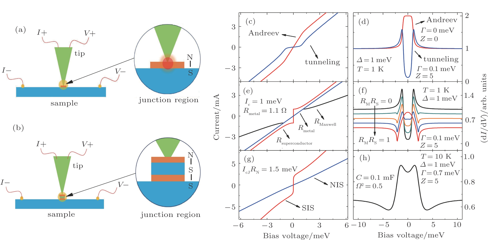
(color online) Response of a point-contact when critical current effects are accounted for. (a) and (b) Schematics of the typical assembly for point-contact spectroscopy measurements, where a tip is brought into contact with the sample. The current I (I+ and I−leads) is measured as a function of the bias voltage V (V+ and V−leads). The enlargement of the contact region shows the simplified structure described in the theoretical model: (a) an N/I/S junction with heating and (b) an N/I/S junction in series with a Josephson junction (S/I/S). N, I, and S stand respectively for normal metal, insulator and superconductor. (c) Typical I(V) dependence of the N/I/S junction calculated with the BTK model in two extremes regimes: Andreev reflection (red) and tunneling (blue). (d) Differential conductance
d
I
/
d
V
(
V
)
spectra corresponding to the curves in panel (c). Here Γ represents the decay of finite quasi-particle lifetime by inelastic scattering. (e) Typical I(V) dependence of the Maxwell resistance RM (black) considering the contributions of the metallic tip and the superconducting sample (red). (f) Differential conductance
d
I
/
d
V
(
V
)
spectra for several
R
M
/
R
S
ratios. (g) Contributions of the N/I/S (blue) and S/I/S (red) junctions to the total resistance of the junction represented in panel (b). (h) Differential conductance
d
I
/
d
V
(
V
)
spectra corresponding to the curves in panel (g).
|