

Transport properties of mixing conduction in CaF2 nanocrystals under high pressure
Cite this Article
Hu Ting-Jing, Cui Xiao-Yan, Wang Jing-Shu, Zhang Jun-Kai, Li Xue-Fei, Yang Jing-Hai, Gao Chun-Xiao. Transport properties of mixing conduction in CaF2 nanocrystals under high pressure. Chinese Physics B, 2018, 27(1): 016401 
Permissions
Transport properties of mixing conduction in CaF2 nanocrystals under high pressure
† Corresponding author. E-mail:
Abstract
We report on the intriguing electrical transport properties of compressed CaF2 nanocrystals. The diffusion coefficient, grain and grain boundary resistances vary abnormally at about 14.37 GPa and 20.91 GPa, corresponding to the beginning and completion of the Fm3m–Pnma structural transition. Electron conduction and ion conduction coexist in the transport process and the electron conduction is dominant. The electron transference number of the Fm3m and Pnma phases increases with pressure increasing. As the pressure rises, the F− ion diffusion and electronic transport processes in the Fm3m and Pnma phases become more difficult. Defects at grains play a dominant role in the electronic transport process.
1. Introduction
Fluoride materials have been studied for a very long time because they have a wide range of potential optical applications based on their low-energy phonons and high ionicity, which result in less absolute fundamental absorption compared with other oxide or sulfide materials.[1–4] As an important class of fluorides, alkaline earth metal fluorides are dielectric materials, which have been widely used in microelectronic and optoelectronic devices, such as wide-gap insulating overlayers, gate dielectrics, insulators, and buffer layers in semiconductor-on-insulator structures and more advanced three-dimensional (3D) devices.[5–8] As an important type of alkaline earth metal fluoride, calcium fluoride (CaF2) has become the focus of the semiconductor industry with the development of UV-lithography due to its high transmittance and low absorption coefficient.[9,10] CaF2 can replace fused silica because it possesses a high laser-induced damage threshold and high transparency until the vacuum ultraviolet region. Therefore, it is considered as the optimal material for deep ultraviolet laser lithography techniques.[11]
With the development of nanometer materials, inorganic nanoscale fluorides are going to play an essential role in various applications based on their unique optical, electrical, and magnetic properties. As a typical anionic conductivity material, the conductive property of CaF2 is an interesting subject. In 1995, Puin et al. measured the conductivity of nanocrystalline CaF2 and found that the F− ionic conductivity in nanophase fluorides increases greatly, in contrast to that in the corresponding single crystalline phase.[12] Boulfelfel et al. predicted that superionic conduction would emerge in the phase interfaces of the fluorite-to-cotunnite transition of CaF2.[13] Despite there being many high-pressure studies regarding the phase transitions of CaF2,[14–17] very few experimental and theoretical works have reported its charge transport behavior under high pressure.
In this work, we conducted a comprehensive investigation on the high-pressure electrical transport properties of CaF2 nanocrystals by using in situ alternate-current (AC) impedance spectra measurements in a diamond anvil cell (DAC) at up to 30.0 GPa. In addition, the variations of diffusion coefficient, bulk and grain boundary resistances with pressure were also discussed.
2. Experimental section
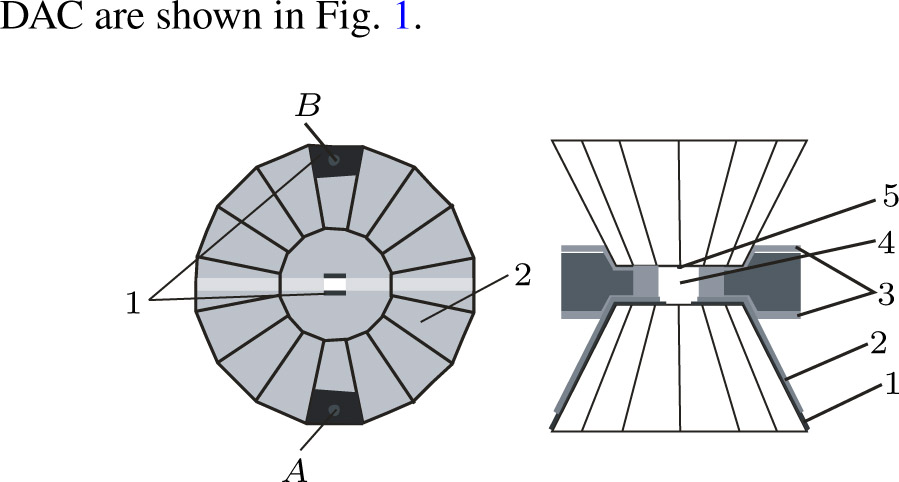
High pressure was conducted by using a Mao–Bell-type diamond anvil cell. The culet of the diamond anvil was 
 | Fig. 1. (a) Completed microcircuit on diamond anvil and (b) the profile of our designed DAC. 1 is Mo, 2 is an alumina layer, 3 is an insulating layer, 4 is the sample chamber, and 5 is ruby. A and B are the contact ends of the microcircuit. |
A T301 stainless steel was used as a gasket that was pre-indented into 


3. Results and discussion
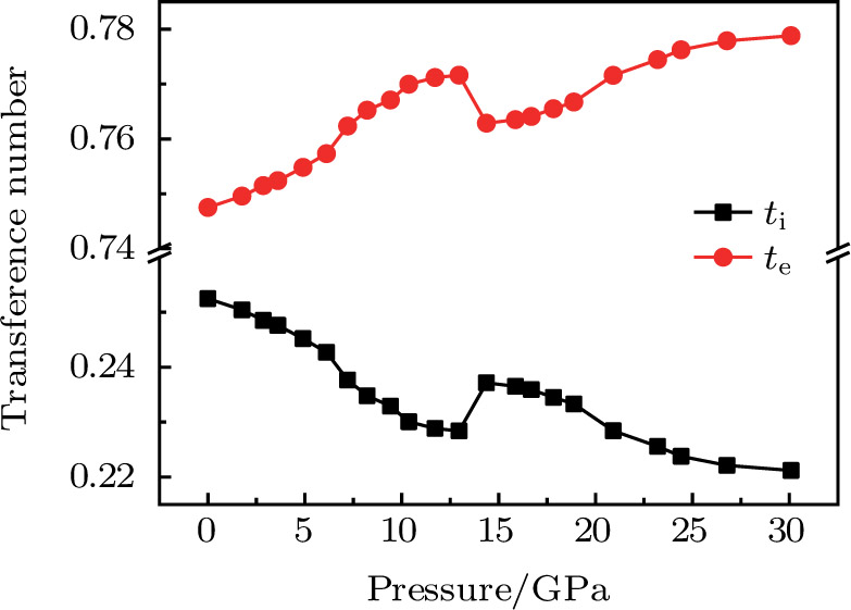
4 ). Figure 6 shows the variation of ion and electron transference numbers with pressure. It can be seen that the transference numbers of ion and electron change discontinuously at about 14.37 GPa and 20.91 GPa. According to our previous XRD results,[21] under compression the Pnma structure appears in the Fm3m phase at about 14.0 GPa. However, the transition is rather sluggish, and both the low-pressure and Pnma phases co-exist up to a pressure of 22.2 GPa.[21] Therefore, the discontinuous changes of ion and electron transference numbers should be caused by the Fm3m–Pnma phase transition of CaF2 nanocrystals under high pressure. In the whole pressure region, the electron conduction has the dominant contribution to the transport process of CaF2 nanocrystals, and the electron transference number of the Fm3m and Pnma phases increases as the pressure rises.
Figure 


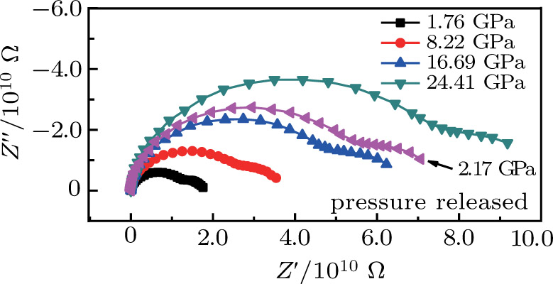
 | Fig. 2. (color online) The 

|
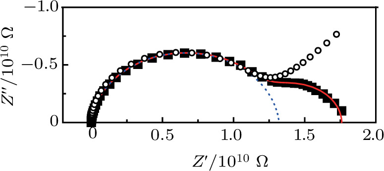
To deeply analyze the impedance spectroscopy, the obtained data are usually modeled by an equivalent circuit. The ionic conduction of F− can be revealed by the 


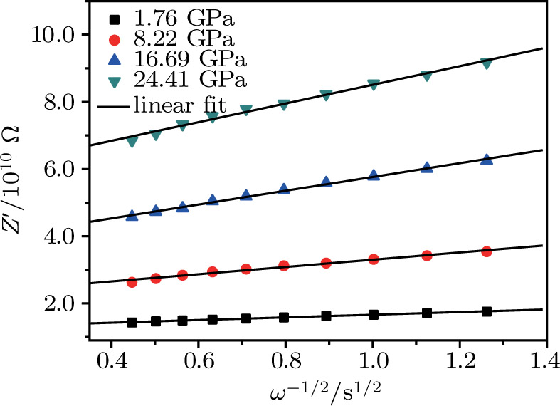 | Fig. 3. (color online) The 

|
From Fig. 


 | Fig. 4. (color online) The 

|
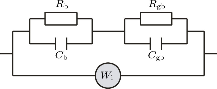
Thus, electron conduction and ion conduction coexist in the transport process of CaF2 nanocrystals. We used the equivalent circuit in Fig.
 | Fig. 5. The equivalent circuit model for mixing conduction of electron and ion. 


|
From Fig.
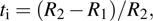
Because F− ions and electrons coexist in CaF2 nanocrystals, it is necessary to distinguish each carrier contribution to the transport process. The transference number[22] is usually used to describe the contribution of each type of carrier to the transport process. The F− ion transference number (

 | Fig. 6. (color online) The variation of ion and electron transference numbers with pressure. |
Due to the existence of the ionic conduction, in the low frequency region 


The ion diffusion coefficient can be expressed as

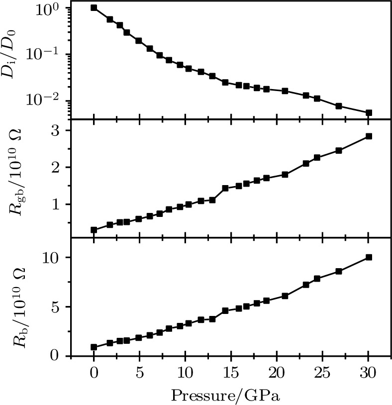 | Fig. 7. The pressure dependence of (a) diffusion coefficient, (b) grain resistance, and (c) grain boundary resistance of CaF2 nanocrystals. D0 is the diffusion coefficient at 0 GPa. |
Using the equivalent circuit model (Fig. 

From Fig.
In the Fm3m and Pnma phases, the diffusion coefficient of the F− ion decreases, whereas the grain resistance and the grain boundary resistance increase as the pressure rises; which indicates that both the F− ions diffusion and electronic transport become more difficult under compression. In the whole pressure range, the grain resistance is larger than the grain boundary resistance, which indicates that the grain resistance has a major contribution to the total resistance and defects at grains play a dominant role in the electronic transport process.
4. Conclusions
The electrical transport properties of CaF2 nanocrystals have been investigated by in situ impedance measurement up to 30 GPa. Each parameter changes discontinuously at about 14.37 GPa and 20.91 GPa, corresponding to the beginning and completing of CaF2 nanocrystals phase transition under high pressure. Electron conduction and ion conduction coexist in the transport process and the electron conduction is dominant. The electron transference number of the Fm3m and Pnma phases increases with pressure increasing. As the pressure rises, the F− ion diffusion and electronic transport processes in the Fm3m and Pnma phases become more difficult. Defects at grains play a dominant role in the electronic transport process.
Reference
| [1] | |
| [2] | |
| [3] | |
| [4] | |
| [5] | |
| [6] | |
| [7] | |
| [8] | |
| [9] | |
| [10] | |
| [11] | |
| [12] | |
| [13] | |
| [14] | |
| [15] | |
| [16] | |
| [17] | |
| [18] | |
| [19] | |
| [20] | |
| [21] | |
| [22] |