1. IntroductionA variable optical attenuator (VOA) is used for gain equalization in dynamic channel-power and wavelength-division multiplexed cross-connect nodes[1,2] in telecommunication applications. Among all kinds of VOAs that have been invented,[3–6] a silica-based planar lightwave circuit (PLC) is an advantageous platform of integrating various photonic devices,[7,8] such as coupler based devices, arrayed-waveguide grating (AWG) multiplexers,[9,10] and thermo-optic switches. This optical integration drastically reduces both device size and assembly cost by eliminating the need for interconnecting fibers between individual circuits.[11] Unfortunately, high power consumption due to the low thermo-optic coefficient of silica[12] has affected the wide applications of the PLC-VOA. The power consumption of PLC-VOA reported in the former paper was mostly greater than 200 mW.[11,13] But in ROADM[14] and multi-channel V-AWG,[15] it is required that the power consumption of the VOA should be less than 150 mW. Although the VOA based on SOI has a very low power consumption, it has a larger coupling loss when coupled with an optical fiber.
Generally speaking, the problem of large power consumption in PLC-VOA can be solved by forming heat-insulating grooves beside both sides of the waveguide. These grooves can serve as a heat insulator and reduce the power consumption because air has much smaller thermal conductivity than SiO . But the power consumption is still higher than 200 mW. Another better method is to use suspended narrow ridge structures,[16] but this will complicate the fabrication process. Although the method of forming grooves has been put forward to solve the problem, how to optimize the geometry of the grooves and the waveguide has not been researched.
In this paper, we use the finite-element analysis to simulate the thermal distribution of the structure under the guidance of these methods and further optimize the performance of the VOA. Besides, in the practical application, the driving voltage is an important parameter and should be lower than 5 V in general. We could optimize the thickness and materials of the electrode.
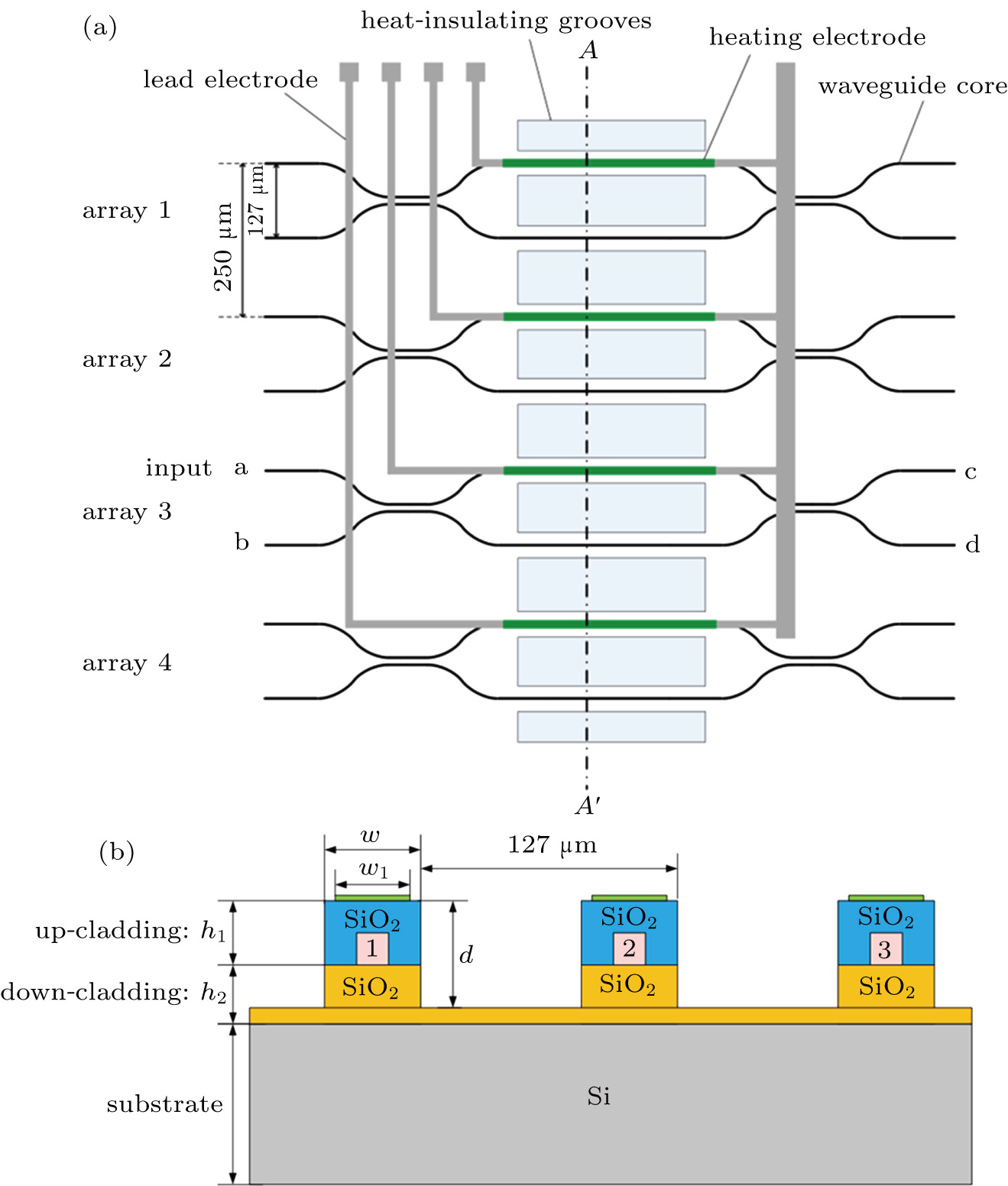
2. Thermal simulations of the PLC-VOAA schematic configuration of the conventional 4-channel PLC-VOA array is illustrated in Fig. 1(a). The spacing between two adjacent VOAs is 250 μm. In Fig. 1(a), the black line represents the waveguide core, the green part represents the heating electrode, and the gray part represents the lead electrode. The rectangular boxes between different arms represent the heat-insulating grooves. The conventional VOA consists of a Mach–Zehnder interferometer (MZI), which has two 3-dB directional couplers and two waveguide arms with thin film heaters on their surfaces. If a beam of light is input by the single-mode input waveguide port a, it is divided into two beams of equal intensity after the directional coupler. Then the two beams of light spread along the two waveguide arms respectively. When the two phase-shifter arms are completely symmetrical, the two divided beams are recombined interferometricly in the output waveguide port d with the constant intensity as the input. As a VOA, the output light intensity depends on the relative phase of the two beams at the second coupler. The average output after the interference is
 | |
where

is the phase difference of the two beams. When the phase difference changes from 0 to

, the output light intensity of port d will reduce from the maximum to the minimum. The maximum power consumption occurs when the output light intensity of port d is the minimum or when the phase shift

is realized
where

is the wavelength 1.55 μm,

is the thermo-optic coefficient of SiO

,

is the temperature difference between the two arms, and
L is the length of the phase-shift arm. The phase difference can be introduced by making the lengths of the two waveguide arms different or changing the refractive index difference via the thermal-optic effect.
In order to establish the model of thermal analysis, the cross-sectional view of the PLC-VOA is shown in Fig. 1(b). The thickness of the up-cladding is  and the thickness of the down-cladding is
  . The etching depth of the grooves is d. The cladding ridge width is w. The width of the heating electrode is
  . The width of the insulating grooves changes with the change of w. The thickness of the substrate is a constant, 625 μm. L and
  are 4000 μm and 21 μm respectively. The distance between the adjacent arms is 127 μm. We assume that core 2 is under control and the electrical power is supplied to it. The temperature of all the cores is monitored. The thermo-optic coefficient of SiO
 is
is  K
K and the thermal conductivity is
  . The required temperature difference
  to implement
  phase shift is
So the needed temperature difference is 16 °C.
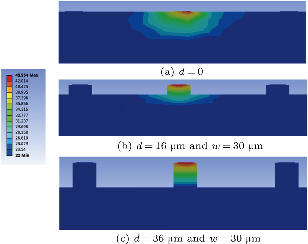
During the analysis, the back surface of the silicon wafer is set at the room temperature (22 °C). The heat flow in the finite-element analysis is supplied to core 2. The thermal field distribution is shown in Fig. 2. The colors of core 1 and core 3 in the thermal field diagram are always dark blue, the same as that of the substrate. That is to say, the temperature of core 1 and core 3 is almost the same as the room temperature (22 °C) while the parameters that we consider are changing. This is mainly because the thermal conductivity of the substrate silicon is much larger than that of silica and the grooves are wide enough so that the heat between different arms is isolated completely. Based on the above discussion, the  phase shift is realized when the temperature of core 2 reaches 38
  C. We consider this as a reference in the simulation.
Firstly, we consider the influence of the etching depth d on  , where
  ,
,  , and w are set to be 16 μm, 20 μm, and 30 μm, respectively. The thermal field distributions with d being 0, 16 μm, and 36 μm are shown in Figs. 2(a)–2(c). The temperature of core 2 is 31.94 °C, 36.45 °C, and 43.4
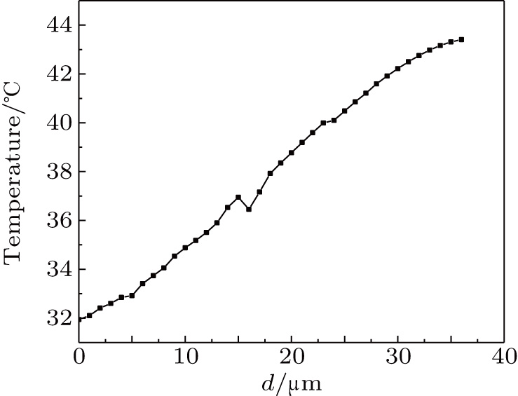
  C in Figs. 2(a)–2(c), respectively. The energy in Fig. 2(b) is more focused on the core 2 area compared to that in Fig. 2(a) without the heat-insulating grooves. The energy in Fig. 2(c) is mostly focused on the core 2 area among the three distributions shown. So the structure in Fig. 2(c) has the lowest power consumption. We monitor the temperature of core 2 when the heat flow is 150 mW with different depths of the grooves. The simulation result is shown in Fig. 3. The temperature of core 2 increases when the grooves are deeper, that is, the power consumption reduces with the increase of the depth. The slope of the fitted curve is 0.35 °C/μm. There is a break point at
  m. The temperature of core 2 further increases after d exceeds 16 μm. The maximum depth is obtained when all the claddings are etched away. Though the substrate Si could be etched as well, we choose not to because this will enhance the difficulty of the fabrication process. We use the maximum depth of the grooves in the following simulation and experiment.
Secondly, we consider the influence of  on the power consumption, where
  and w are set to be 16 μm and 30 μm, respectively. The simulation result is shown in Fig. 4(a). With the increase of
  , the power consumption decreases. The slope of the fitted curve is 5.92 mW/μm. But the down-cladding thickness
  cannot increase without limit, because the oxidation rate goes down with the increase of the oxide layer thickness. Considering the oxidation time, the maximum thickness that we can achieve is 22 μm under the condition of the current fabrication process.
Thirdly, we consider the influence of  on
on  , where
  and w are set to be 20 μm and 30 μm, respectively. Based on the results shown in Fig. 4(b), the temperature of core 2 reduces as
 increases when the power supply is 150 mW. In other words, the power consumption increases with the increase of
  . However, the influence of
  to the temperature is 0.017 °C/μm, which is so small that we can ignore the influence in practical application. Hence, we adopt
  as a constant of 16 μm in the actual manufacturing process.
The minimum cladding thickness can be calculated by the Goos-Hanchendisplacement formula
where
X is the penetration thickness,

is the wave number in the vacuum,

is the mode refractive index of the core fundamental mode, and

is the refractive index of the cladding.

0 for the TE mode, and

for the TM mode. The penetration thicknesses of the TE and TM modes can be calculated as

m and

m, respectively. As a matter of fact, it is usual to take 5–8 times of this value. So the minimum thickness of the up-cladding is selected as 16 μm. This thickness can effectively prevent light leakage from the waveguide core to the cladding and also prevent the absorption of the optical signals by the metal film in the core. It can guarantee that the light transmission of the waveguide core is not affected.
Finally, we consider the influence of w on the power consumption, where  and
and  are set to be 16 μm and 20 μm, respectively. In Fig. 4(c), we find that the power consumption reduces when w decreases and the slope of the fitted curve is 3.87 mW/μm, so we cannot neglect this influence. The cladding ridge width cannot be too narrow in order to prevent light leakage in both sides.
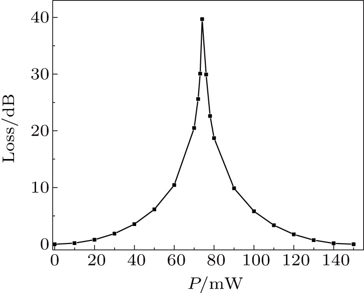
According to the above discussion, the structure that has the lowest power consumption should have up-cladding thickness 16 μm, down-cladding thickness 22 μm, and cladding ridge width 21 μm. Based on the above parameters, we give the simulation result of insertion loss versus power consumption, as shown in Fig. 5. The temperature of core 2 under different power can be obtained by the finite-element analysis. Then the phase difference  can be calculated through formula (2). Finally the insertion loss is obtained through formula (1). The simulated power consumption of this structure is about 74 mW, which is supplied to the heating electrode. In the experiment, this value would be larger because a portion of the power is dissipated on the lead electrode.
In addition, the influence of the driving voltage should also be considered. We assume that the power consumption is 150 mW and the driving voltage is 5 V, then the resistance of the heating electrode should be 166  according to the power versus voltage formula
  . In theory, the resistance can be calculated by the formula
  , where
  is the electrical resistivity, l is the length, and s is the sectional area of the resistance. The resistance of the lead electrode should be far smaller than that of the heating electrode in order to make full use of the power, that is, most of the power is supplied to the heating electrode. The common materials for the heating electrode are Ti or Wu and the common materials for the lead electrode are Al, Cr, or Au. Among them, Ti and Cr have the effect of adhesion to the chip. We choose Ti and Wu as the heating electrode, and Cr and Al as the lead electrode because Ti and Wu have larger electrical resistivity than Cr and Al. So the heating electrode is 50 nm Ti and 500 nm Wu, the lead electrode is 30 nm Cr and 1200 nm Al.
3. Experimental results and discussionWe fabricated a 4-channel silica-based VOA array based on the results above. The silica-based waveguides were fabricated by a combination of thermal oxidation, PECVD, photolithography, and reactive ion etching. The heating and lead electrodes were formed on the waveguide by magnetron sputtering. The geometry of the waveguide is as follows:  m,
m,  m, 22 μm,
  m, 24 μm, 27 μm, 30 μm, 35 μm. The depth of the grooves is the maximum. The refractive index difference between the core and the cladding is 0.75%. The core is 6 μm
 m in size.
The resistances of the heating and the lead electrodes are approximately 140  and 15
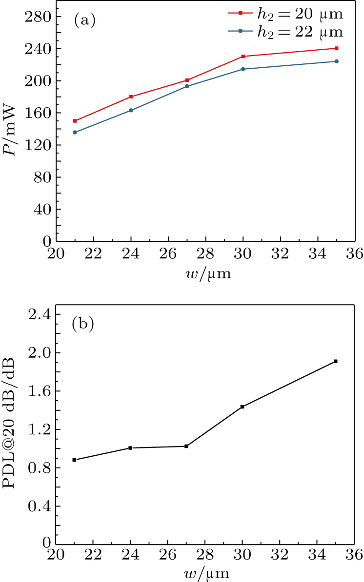
  , respectively. The driving voltage is about 4.5 V, which meets our demand. Figure 6(a) shows the power consumption versus the cladding ridge width with different
  . The power consumption at an attenuation of 30 dB ranges from 135 mW to 224 mW when
  is 22 μm. The power consumption of the down-cladding thickness 22 μm is less than that of the thickness 20 μm, which is consistent with the theoretical analysis. The minimum power consumption is 135 mW, which is larger than the simulation result of 74 mW. This may be because the thermal parameters of the materials we use in the simulation are slightly different from the actual ones. But the changing trends of the simulation and the experimental results are the same, so the simulation results can point out the correct direction for improvement in the experiment. The average insertion loss is 0.7 dB. The PDL value at an attenuation of 20 dB ranges from 0.882 dB to 1.91 dB as shown in Fig. 5(b). The width of the cladding ridge is narrower, and the PDL is lower.
Figure 7 shows the characteristics of the fabricated 4-channel variable optical attenuator array when w is 21 μm. Figure 7(a) shows the insertion loss versus the applied power superimposed over 4 channels. The power consumptions at an attenuation of 30 dB are 135.38 mW, 144.9 mW, 143.25 mW, and 153.2 mW, respectively. It confirms that the power consumption is stably suppressed to less than 155 mW through 4 channels. The trend of the four curves is similar to that in Fig. 5. Figure 7(b) shows the insertion loss versus the applied electrical voltage. The driving voltages at an attenuation of 30 dB are 3.1 V, 3.5 V, 3.5 V, and 4.1 V, respectively. The driving voltage is successfully reduced to less than 5 V, which thanks to the excellent metal film sputtering process. Because the lengths of the lead electrodes are different, the power consumptions and driving voltages of the 4 channels are slightly different.


