† Corresponding author. E-mail:
Two kinds of InAs/GaAs quantum dot (QD) structures are grown by molecular beam epitaxy in formation–dissolution–regrowth method with different in-situ annealing and regrowth processes. The densities and sizes of quantum dots are different for the two samples. The variation tendencies of PL peak energy, integrated intensity, and full width at half maximum versus temperature for the two samples are analyzed, respectively. We find the anomalous temperature dependence of the InAs/GaAs quantum dots and compare it with other previous reports. We propose a new energy band model to explain the phenomenon. We obtain the activation energy of the carrier through the linear fitting of the Arrhenius curve in a high temperature range. It is found that the GaAs barrier layer is the major quenching channel if there is no defect in the material. Otherwise, the defects become the major quenching channel when some defects exist around the QDs.
Semiconductor quantum dot (QD) lasers have attracted considerable attention as the most promising light sources for future communication, owing to their low threshold current densities, high temperature stabilities,[1–3] longer wavelengths, high modulation speeds, and low chirps.[4–7] The performances of the QD lasers are directly related to the optical properties of the QD materials.[8] Photoluminescence (PL) spectroscopy is an effective technique to characterize the optical properties of the QD materials. In particular, by analyzing the PL spectrum variations with temperature, we can deduce the quenching channel of QD material.[9–11] Thermionic emission of the photo-excited carriers out of the QD potential was found to be a dominant mechanism leading to the thermal quenching of the PL in self-assembled quantum dots (QDs).[9,10,12,13] Xu et al.[11,14] grew a number of self-organized InAs/GaAs heterostructures with InAs layer thickness values from 0.5 ML to 3 ML, then investigated the temperature dependence of PL properties of the samples. They found that for InAs mono-layers or sub-mono-layers the barrier for the thermionic emission of carriers is GaAs, while for high-quality InAs multi-layers the wetting layer might serve as a barrier. Dai et al.[15] found that the emission intensity quenched rapidly when the temperature rose to around 60 K, indicating the existence of defect-related center in the vicinity of InAs/GaAs interface. They suggested that the PL quenching was dominated by defect-related centers instead of GaAs in their case. Huang et al.[16] grew extremely low density InAs QDs by molecular beam droplet epitaxy. They deposited a proper amount of gallium (Ga) to saturate the excess As atoms that were present on the substrate surface. Then In atoms were deposited on the GaAs buffer layer, forming InAs QDs. No wetting layer connecting the QDs was observed, and no typical temperature-related PL properties of QDs formed by the Stranski–Krastanov (S-K) growth mode were shown either. The peak energy did not show super-fast redshift and the full width at half maximum (FWHM) did not transform with the temperature increasing either. It meant that wetting layer was the transfer channel of carriers in regular S-K QDs.
In this paper, we report a formation–dissolution–regrowth[17] (FDR) method to fabricate low-density, longer-wavelength InAs/GaAs QDs, for the future application in single-photon light sources in fiber-based quantum communication.[18–26] The temperature dependence of PL peak energy, intensity, and FWHM of the samples were studied. We found that it was different from the results reported previously.[9,10]
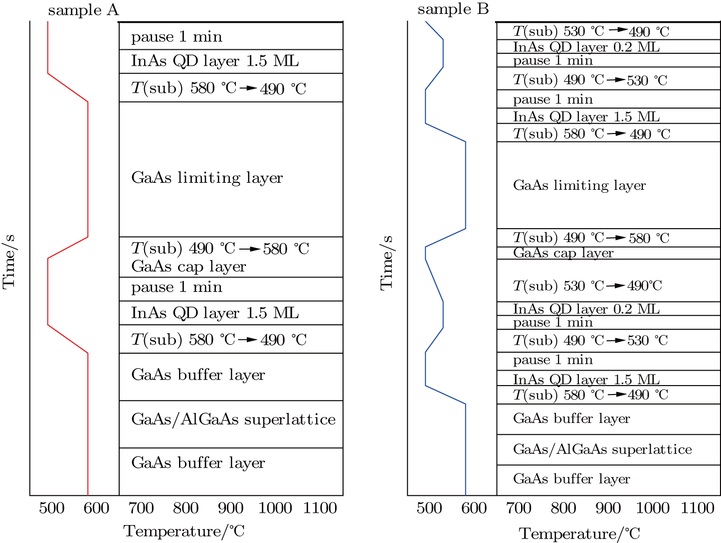
Two kinds of samples were grown on GaAs (100) substrates in a Veeco Mod GenII solid-source molecular beam epitaxy (MBE) system. A 100-nm GaAs buffer layer, a GaAs/AlGaAs superlattice, and another 100-nm GaAs layer were grown consecutively at 580 °C as shown in Fig.
Thereafter, a 15-nm GaAs cap layer was grown on the InAs QD layer at 490 °C, and a 285-nm GaAs was grown at 580 °C for both samples.
Finally, we grew a surface InAs quantum dot layer on the top of GaAs for each sample in the same way as for the buried quantum dot layer, in order to observe the quantum dot morphology.
The surface morphology was imaged by a Solver P47 atomic force microscope (AFM) system. Photoluminescence (PL) measurements were performed using a Fourier transform infrared spectrometer equipped with an InGaAs detector. Both samples were excited by a 532-nm solid-state laser and mounted in a cryostat providing temperatures from 15 K to 300 K.
In Fig.
Owing to the larger QD size in sample B, the PL wavelength of sample B is considerably longer than that of sample A, reaching the 1.3 μm (0.95 eV) window of fiber communication as indicated in Fig.
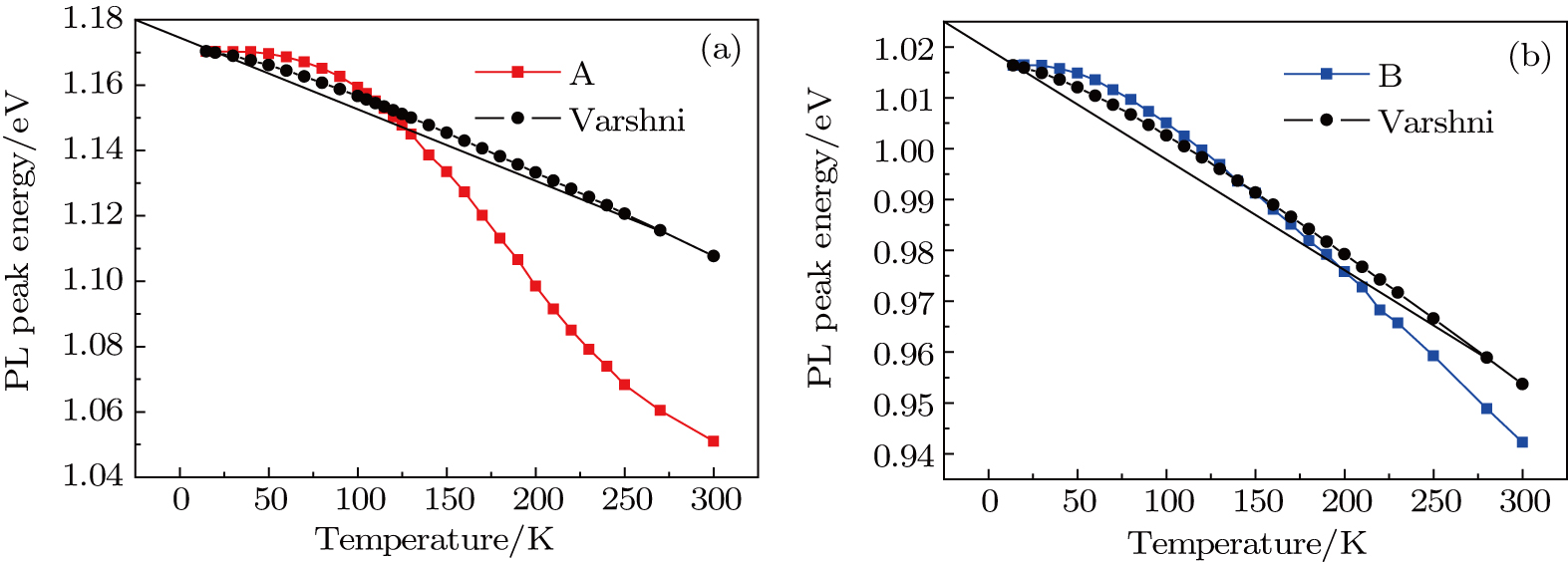
 | Fig. 3. (color online) Plots of PL peak energy and Varshni value versus temperature for samples A and B. |
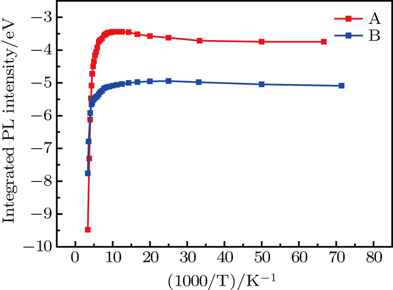
The temperature dependence of PL peak energy, intensity, and FWHM for samples A and B are measured and summarized in Figs.
We analyze the relationship between experiment value of PL peak energy and theoretical Varshni value. The equation of Varshni[30] describes the theoretical PL peak energy versus temperature, which is
 |


Focusing on the low temperature part (
 | Fig. 4. (color online) Temperature dependence of energy difference between experimental value and Varshni value (a), integrated PL intensity (b), FWHM of PL spectra (c) for sample A. |
To explain the phenomena in the low temperature part of the curves, we propose an energy band model as illustrated in Fig.
QDs in sample A are prepared by 1.5-ML low-temperature InAs deposition followed by a growth-interruption or in situ annealing at 490 °C, and reveal the dual-mode size distribution as shown in Fig.
With the above model, the temperature dependence of PL from sample A, especially the low temperature part, can be explained as follows.
When 
When 


From the Arrhenius equation
 |


 | Fig. 6. (color online) Arrhenius plots of the temperature dependence of the integrated PL intensity for samples A and B |
When 

To conclude, the existence of the WL2 barrier in sample A causes more carriers to be able to arrive at SQDs at increased temperatures in the 
For sample B, the experimental peak energy is also higher than the Varshni value, and FWHMs go higher with increasing temperatures in the low temperature region of the curves as shown in Figs.
 | Fig. 7. (color online) Temperature-dependent energy difference between experimental value and Varshni value (a), integrated PL intensity (b), FWHM of PL spectra (c) for sample B. |
These phenomena can also be explained by the above energy band model, with the supplementation of a defect energy level (DEF).
QDs in sample B are prepared by 1.5-ML low-temperature InAs deposition followed by an interruption/in-situ annealing at a higher temperature of 530 °C, and the regrowth of 0.2-ML InAs at the same temperature. The density of dots is much lower, and their size is more uniform as illustrated in Fig.
The defect energy level can be located from Fig. 
When 

When 
When the quenched carriers are more than the carriers injected into the SQDs, PL intensity will decrease. The quenching of LQD emission may cause the FWHM to tend to decrease, but the effect of filling of the SQDs will be dominant, so the FWHM increases gradually.
When 
When 
In short, the existence of WL2 barrier in sample B causes more carriers to be able to arrive at SQDs with temperature increasing in the 


In order to develop low-density, longer-wavelength InAs/GaAs QDs for the applications in single-photon light sources in fiber-based quantum communication, we study the temperature dependence of PL peak energy, intensity, and FWHM of two kinds of InAs/GaAs QD samples grown by MBE in formation–dissolution–regrowth method with different in-situ annealing and regrowth processes. It is found that the wetting layer around smaller QDs is thinner than elsewhere, and serves as an energy barrier for the carriers to be injected into small QDs. This gives rise to the anomalous temperature dependence of PL spectrum in a low temperature range, including slower redshift, increase in intensity and FWHM.
It is also found that some defects may be formed around the large QDs and in the long-time high-temperature interruption/annealing during growth. The defect energy level will act as a major quenching channel of PL peak intensity instead of GaAs barrier layer in this kind of sample. So the FDR growth process needs to be further optimized to reduce these defects.
| [1] | |
| [2] | |
| [3] | |
| [4] | |
| [5] | |
| [6] | |
| [7] | |
| [8] | |
| [9] | |
| [10] | |
| [11] | |
| [12] | |
| [13] | |
| [14] | |
| [15] | |
| [16] | |
| [17] | |
| [18] | |
| [19] | |
| [20] | |
| [21] | |
| [22] | |
| [23] | |
| [24] | |
| [25] | |
| [26] | |
| [27] | |
| [28] | |
| [29] | |
| [30] | |
| [31] |


