† Corresponding author. E-mail:
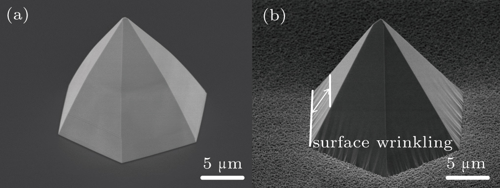
GaN micro-pyramids with AlGaN capping layer are grown by selective metal–organic–vapor phase epitaxy (MOVPE). Compared with bare GaN micro-pyramids, AlGaN/GaN micro-pyramids show wrinkling morphologies at the bottom of the structure. The formation of those special morphologies is associated with the spontaneously formed AlGaN polycrystalline particles on the dielectric mask, owing to the much higher bond energy of Al–N than that of Ga–N. When the sizes of the polycrystalline particles are larger than 50 nm, the uniform source supply behavior is disturbed, thereby leading to unsymmetrical surface morphology. Analysis reveals that the scale of surface wrinkling is related to the migration length of Ga adatoms along the AlGaN 
AlGaN and the relevant III–N compound semiconductors are considered to be ideal materials of light-emitting diodes (LEDs), laser diodes (LDs), and photodetectors covering the ultraviolet (UV) region due to their direct energy band gaps ranging from 3.4 eV to 6.2 eV.[1–4] The wide adjustable emission range of AlGaN-based opto-electrons has a great many applications in water purification, disinfection/sterilization, medicine, and biochemistry.[5,6]
Although the AlGaN epitaxial growth has already been studied for several years, it is still a challenge to grow high-quality, thick AlGaN epilayers with low threading dislocation (TD) density.[7,8] In addition, the conventional devices on c-plane AlGaN are strongly affected by spontaneous and piezoelectric polarization. Therefore, the hexagonal AlGaN micro-pyramid prepared by selective area growth (SAG) technique is thought as a kind of promising building block for reducing the TD[9,10] and suppressing the undesirable polarization effect.[11,12] Although high quality GaN pyramid has been successfully realized by SAG technology in a metal–organic–vapor phase epitaxy (MOVPE) system,[13–15] the SAG of AlGaN pyramids has been a challenge so far because Al adatoms cannot diffuse along a long distance and it is easy to form the nucleation of AlGaN spontaneously on dielectric surface in the environment of nitrogen due to the high bond energy of Al–N.[16] Thus, it is difficult to realize a hexagonal AlGaN micro-pyramid at the mask openings grown by selective area MOVPE, particularly for the high Al composition. But, it may be feasible to form AlGaN/GaN hexagonal pyramidal structure when growing an AlGaN capping layer on a GaN pyramid. Several studies have already been conducted, and the AlGaN/GaN micro-pyramid structure with polycrystalline particles on the mask has been obtained.[17–19] However, due to the effects of migration length of Al and Ga adatoms, the scale of pyramid is still small and the composition of AlGaN pyramid is nonuniform. Therefore, it is meaningful to clarify the migration length of adatoms along a specific crystal facet for growing the selective AlGaN pyramid. Besides, during AlGaN epitaxial growth, the surface morphology and the influence of polycrystalline particles on selective growth are seldom discussed, however, they play a key role in determining the quality of the devices performance.[20]
In this work, a thick AlGaN capping layer of AlGaN/GaN micro-pyramid is grown by selective MOVPE and the associated polycrystalline particles are formed on a dielectric mask. It is shown that a large amount of surface wrinkling emerges at the bottom of the AlGaN/GaN micro-pyramid, the length of which changes with Al composition. In order to explain the phenomenon of the surface wrinkling, the model of the source supply during SAG is introduced and the effect of the polycrystalline particles on the mask is discussed. The surface diffusion lengths of Ga adatoms along the 
The AlGaN/GaN micro-pyramids were grown on a patterned template by using a low pressure MOVPE system according to the following steps. An GaN/AlN film with a thickness of 500 nm/100 nm was grown on the cleaned Si substrate at 1095 °C, which served as a seeding layer for subsequent re-growth. Then, the wafer was taken out from the reactor chamber and a 100-nm-thick SiO2 was deposited on the seeding layer by plasma-enhanced chemical vapor deposition (PECVD). Afterwards, the SiO2 mask layer was patterned by conventional photolithography technique and the circle window used as SAG was opened by selective wet etching with diameter and period being 5 μm and 60 μm, respectively. After chemical cleaning, the patterned template was reloaded into the MOVPE chamber for re-growth. The GaN micro-pyramids were first grown on the windows for 30 min at 1020 °C, followed by a 1500-nm-thick AlGaN layer formed on the GaN pyramids at 1080 °C.
During the growth, trimethylgallium (TMG), trimethylaluminum (TMA), and NH3 were used as the precursors. The composition content of the AlxGa1−x N alloy was regulated by changing the flux ratio between TMG and TMA. The surface morphology of the AlGaN/GaN micro-pyramid was characterized by scanning electron microscope (SEM Hitachi S-4800) and atomic force microscope (Veeco Dimension Edge) with an acceleration voltage of 5 kV.
Figure 


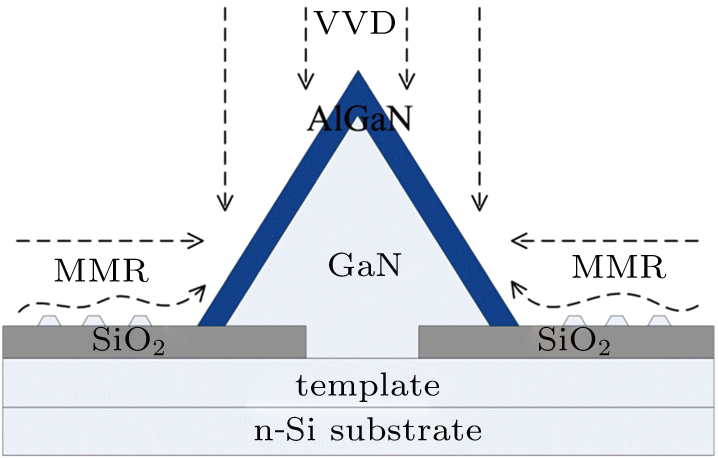
In order to reveal the formation mechanism of the surface wrinkling, source diffusion path for selective MOVPE should be illustrated clearly, particularly when the source is transported near the dielectric surface. In selective MOVPE, two main source supply paths are considered.[21] As illustrated in Fig.
It is noted that epitaxy growth is sensitive to the environment of temperature, ambient gas pressure, and flow of source. When polycrystalline particles grow to a considerable scale, the effect related to source supply in selective MOVPE should be considered. Because of the irregular distribution of AlGaN polycrystalline islands on the mask, the source supply from mask regions to growth regions is disturbed and nonuniform. More specifically, a relatively large polycrystalline island on the dielectric mask will slightly block the source from being supplied from the dielectric mask to the growth region, namely the MMR effect near the mask surface, leaving less source supply to the back of the island and more to the side of the island. Therefore, the nonuniform source supply causes the unsymmetrical growth and some surface wrinkling to emerge spontaneously. However, this nonuniform source supply model does not work for the VVD effect, because the VVD effect can directly push the source to the growth region from the ceiling. Furthermore, the MMR effect is the major source supply to the sidewalls of the AlGaN/GaN micro-pyramids but the VVD effect is the major source supply to top regions. As a result, the surface wrinkling shown in Fig.
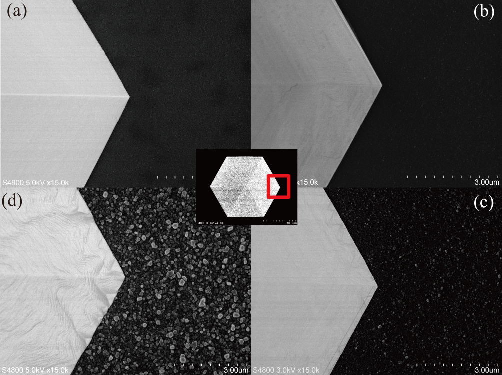
It is shown that when the AlGaN polycrystalline islands on the dielectric mask are large enough, the nonuniform source supply effect becomes obvious. Therefore the scale of the polycrystalline islands and its influence on the pyramids surface must be discussed. Figure
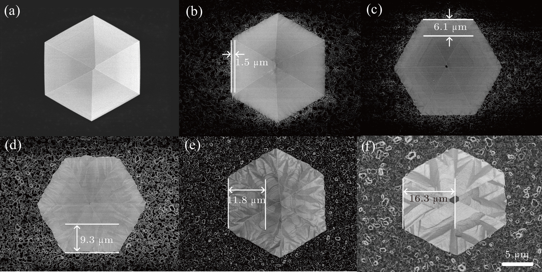
The above analysis reveals that the origination of the surface wrinkling arises from the nonuniform migration behaviors of adatoms. Therefore, the scale of the surface wrinkling represents the interaction area where the nonuniform source can reach from the bottom to the top, which is the migration length along the AlGaN 


The results imply that the migration length of Ga adatoms along the AlGaN 

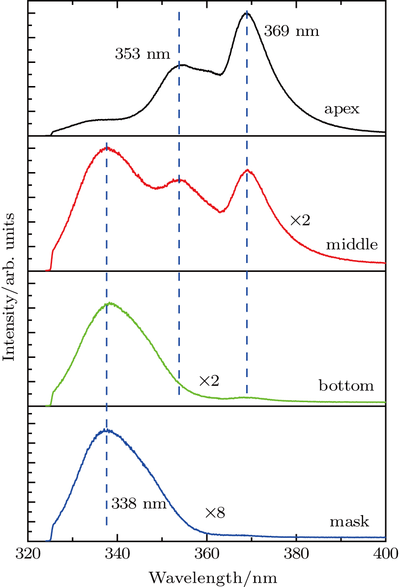
For investigating the compositional uniformity of the AlGaN capping layer, the optical characteristics of the AlGaN/GaN micro-pyramids are obtained by room temperature micro-photoluminescence (μ-PL) measurement. The AlGaN capping layer is grown for 30 min at 1080 °C by supplying 

In this work, AlGaN/GaN micro-pyramids grown by selective MOVPE are studied. It is shown that a large amount of surface wrinkling emerges at the bottom of the AlGaN/GaN micro-pyramid, which is caused by the nonuniform source supply from the dielectric mask region to the growth region when the scale of the polycrystalline particles on the mask is larger than 50 nm. Analysis clarifies that the size of surface wrinkling is related to the migration length of Ga adatoms along the AlGaN 
| [1] | |
| [2] | |
| [3] | |
| [4] | |
| [5] | |
| [6] | |
| [7] | |
| [8] | |
| [9] | |
| [10] | |
| [11] | |
| [12] | |
| [13] | |
| [14] | |
| [15] | |
| [16] | |
| [17] | |
| [18] | |
| [19] | |
| [20] | |
| [21] |


