


Effect of deposited temperatures of the buffer layer on the band offset of CZTS/In2 S3 heterostructure and its solar cell performance
Cite this Article
Yu Jinling, Zheng Zhongming, Dong Limei, Cheng Shuying, Lai Yunfeng, Zheng Qiao, Zhou Haifang, Jia Hongjie, Zhang Hong. Effect of deposited temperatures of the buffer layer on the band offset of CZTS/In2 S3 heterostructure and its solar cell performance. Chinese Physics B, 2017, 26(4): 046802 
Permissions
Effect of deposited temperatures of the buffer layer on the band offset of CZTS/In2 S3 heterostructure and its solar cell performance
† Corresponding author. E-mail:
Project supported by the National Natural Science Foundation of China (Grant Nos. 61574038 and 61674038) and the Natural Science Foundation of Fujian Province, China (Grant No. 2014J05073).
Abstract
The effect of the deposition temperature of the buffer layer In2S3 on the band alignment of CZTS/In2S3 heterostructures and the solar cell performance have been investigated. The In2S3 films are prepared by thermal evaporation method at temperatures of 30, 100, 150, and 200 °C, respectively. By using x-ray photoelectron spectroscopy (XPS), the valence band offsets (VBO) are determined to be 


1. Introduction
The Cu2ZnSnS4 (CZTS) thin film is one of the most promising light absorbing materials which has attracted much research interests recently.[1–4] In highly efficient CZTS solar cells, CdS is usually utilized as a buffer layer.[4–6] However, since Cd is toxic, great effort has been devoted to developing CZTS solar cells with Cd-free buffer layers.[5–7] Being non-toxic, In2S3 is a preferable material to replace CdS as a buffer layer.[5,6] Since conduction band alignment between the p-type CZTS and n-type buffer layers is a key factor to influence the device performance, it is of great importance to investigate the band offset of CZTS/In2S3 heterostructures.[6] Yan et al. investigated the band alignment of different buffer layers, i.e., CdS, Zn(O,S) and In2S3 on CZTS, and they found that the conduction band offset (CBO) of In2S3/CZTS is spike-like with a value of 
2. Experiments
In the experiments, four CZTS/In2S3 heterostructure samples were prepared. The CZTS thin films with a thickness of 800 nm were fabricated on floating glass (FG) substrates by sol–gel method, followed by sulphurization in an N2 + H2S gas atmosphere (with 5% H2S concentration) at 580 °C for one hour.[10] The buffer layers In2S3 with a thickness of 5 nm were deposited onto the CZTS thin films by thermal evaporation method in DMDE-450 deposition equipment. The substrate temperature during the deposition of In2S3 was chosen to be 30 (room temperature), 100, 150, and 200 °C, respectively. In order to make the deposition of such a thin film possible, the substrate and the source material was kept at a far distance of about 22 cm. In order to find out the right amount of source material (In2S3 powder) to deposit an In2S3 film of 5 nm, 30-, 50-, and 100-mg In2S3 powder were used as the source material, respectively, and the corresponding thicknesses of the In2S3 films were determined to be 14, 25, and 49 nm by a step profiler (KLA Tencor D-100). Therefore, to deposit an In2S3 film with a thickness of 5 nm, 5-mg In2S3 powder was used as the source material. Besides, another four In2S3 films with a thickness of 400 nm were also prepared by thermal evaporation method, which were deposited on FG substrates at the four temperatures mentioned above, respectively. The transmittance and reflectance spectra were measured by a Cary 5000-Scan UV-vis-NIR Spectrometer in the wavelength range 350 nm–1200 nm. The XPS measurements were carried out using a ThermoFisher Scientific Escalab 250 electron spectrometer with monochromatic Al Kα (
To fabricate a complete solar cell, an intrinsic ZnO film of 60 nm and an ITO film of 270 nm were deposited on top of the glass/Mo/CZTS/In2S3 (50 nm) stack by sputtering. Then, 100-nm Al metal grids were fabricated by thermal evaporation. The J–V curves of the fabricated CZTS solar cells with the buffer layer In2S3 deposited at different temperatures were measured by a solar simulator with an illumination intensity of 100 mW/cm2 (Oriel 91192, AM1.5, Global).
3. Results and discussion
Here

and

are the energy positions of the valence band maximum (VBM) of CZTS and In2S3 films, and

is the band bending determined by the following expression
where

(

) is the core-level (CL) energy of a selected element in the bulk material of In2S3 (CZTS), and

(

) is the core-level energy of the same element at the heterojunction interface. Then the conduction band offset (VBO) can be obtained by
with

(

) being the energy band gap of In2S3 (CZTS). In this study, we assume that the binding energy below the Fermi energy is positive, and thus a negative VBO (CBO) value indicates a lower valance (conduction) band edge in In2S3 than that in CZTS. The reference CLs in CZTS can be chosen from Cu, Zn, and Sn, and that in In2S3 is adopted to be In. In this work, the final VBO values are determined by averaging the VBO values obtained by using the CL pairs In/Cu, In/Sn, and In/Zn, respectively. Figure 1 shows the valance band spectra of the In2S3 and CZTS films, In 3d core-level spectra of the In2S3 and CZTS/In2S3 (deposited at 150 °C) samples, Zn 2p core-level spectra of the In2S3 and CZTS/In2S3 (deposited at 150 °C) samples, respectively. The VBM values of CZTS and In2S3 are determined to be

eV and

eV, respectively, by extrapolating the linear edges of the valence band spectra to the baseline, as shown in Fig. 1 . The CL positions are obtained by fitting the CL binding energy spectra to Voigt function, a mixed Lorentzian–Gaussian function with a Shirley background, as shown in Fig. 1 . The CL positions in the bulk material and heterostructures deposited at different temperatures are shown in Table 1 , where the CL positions in bulk material are measured in the materials deposited at room temperature, since the CL positions of bulk material do not change with deposition temperatures for the current investigated temperature range. Substituting the CL energies and the VBM values into Eqs. (1 ) and (2 ) and averaging the values obtained by CL pairs In/Cu, In/Sn, and In/Zn, we determine the

to be

,

,

, and

eV, and VBO values to be

,

,

, and

eV for the heterostructures with the buffer layer In2S3 deposited at 30, 100, 150, and 200 °C, respectively, as shown in Table 2 . The

and VBO values of the sample deposited at 30 °C are in good agreement with that reported in Ref. [6] (

:

eV, VBO:

eV) within experimental errors.
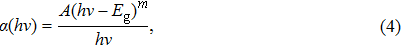
where α is the optical absorption coefficient of the film, A is a constant related to the effective mass, and the value of m indicates different types of transitions, i.e., m = 0.5 stands for allowed direct, 1.5 for forbidden direct, 2 for allowed indirect and 3 for forbidden indirect transitions, respectively. A linear interval cannot be found for the curve of

versus

indicating that the band gap of In2S3 investigated here is not direct. However, a good linear interval can be found in the plot of

versus

, suggesting an indirect band gap of In2S3 films. Thus, the band gap of In2S3 films deposited at 30, 100, 150, and 200 °C are determined to be 2.03, 2.14, 2.01, and 1.92 eV, respectively. It can be seen that the band gap of In2S3 films varies with deposition temperatures. The band gap of CZTS is direct and determined to be 1.45 eV. Then the CBO values are estimated by Eq. (3 ) to be

,

,

, and

eV corresponding to the heterostructures deposited at 30, 100, 150, and 200 °C, respectively, which are also shown in Table 2 .
According to Ref. [11], the valance band offset (VBO) can be calculated using the formula
 |
 |
 |
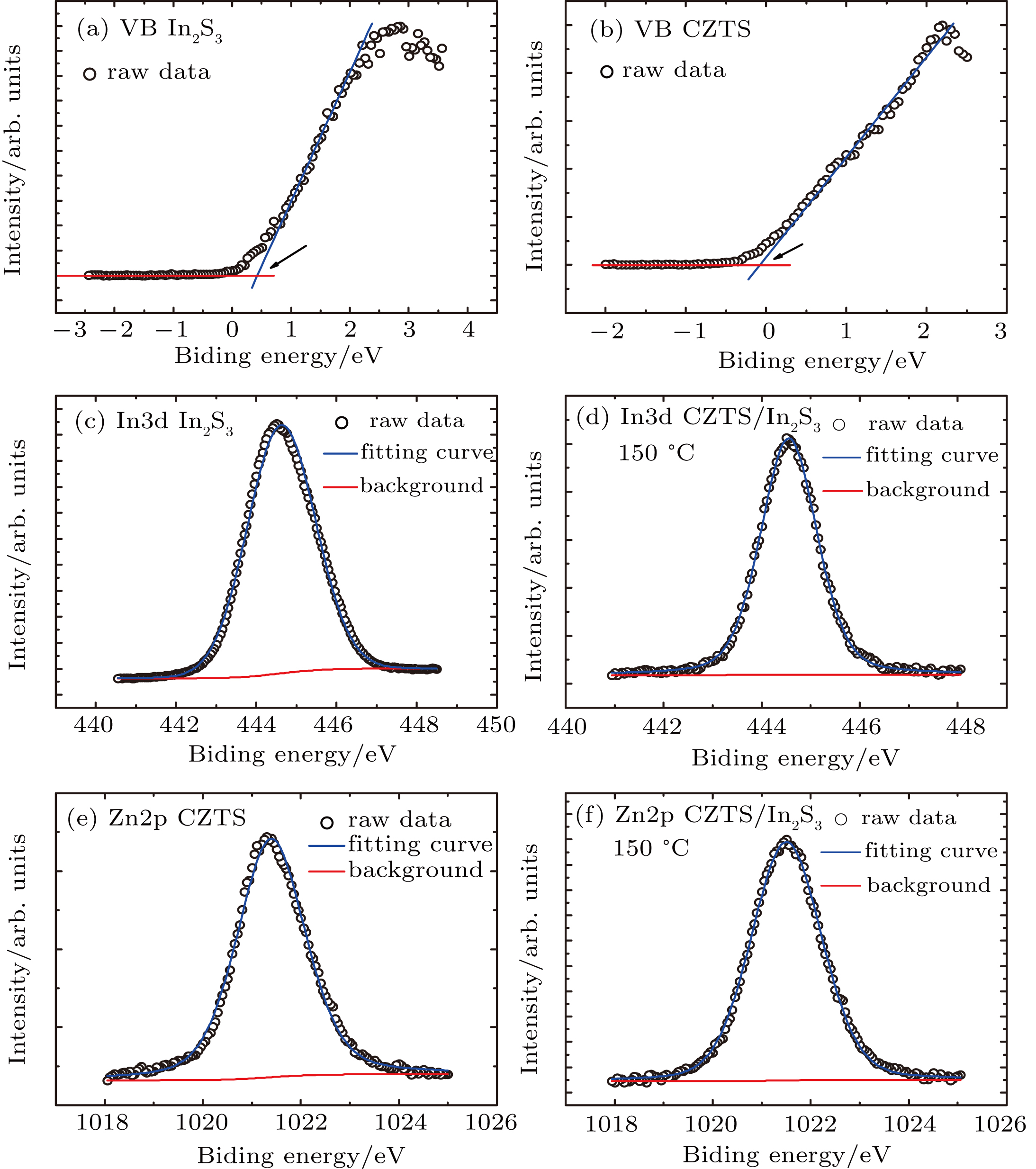 | Fig. 1. (color online) Valance band spectra of (a) the In2S3 and (b) CZTS film samples, (c) In 3d core-level spectra of the In2S3 and (d) CZTS/In2S3 (deposited at 150 °C) samples, (e) Zn 2p core-level spectra of the In2S3, and (f) CZTS/In2S3 (deposited at 150 °C) samples. The VBM positions are determined by extrapolating the linear edges of the VB spectra to the baseline, and the CL spectra are fitted to Voigt function. |
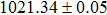
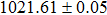
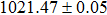
| Table 1.
Core-level energies obtained by the XPS spectra fitting for the bulk In2S3, bulk CZTS, and CZTS/In2S3 heterostructures deposited at different temperatures. . |
| Table 2.
|
The band gap 
 |
The CBO can also be easily calculated by using the Anderson model,[12] if electron affinity χ of In2S3 and CZTS are known. Electron affinity χ of In2S3 and CZTS are estimated to be 

With the values of VBO, CBO, and 
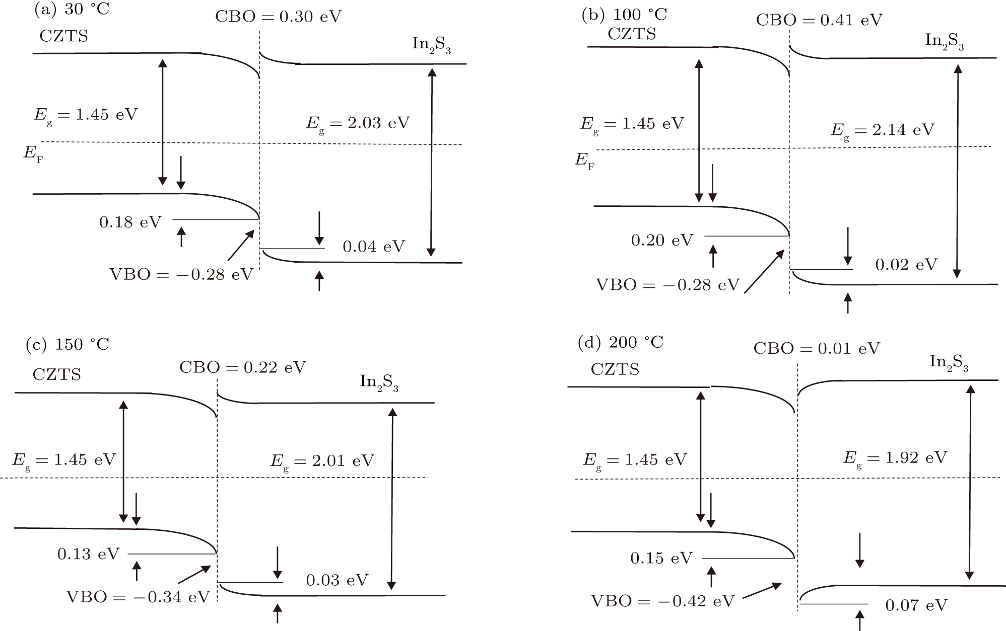 | Fig. 2. Band offset diagram for the heterostructures deposited at different temperatures. |
| Table 3.
Element content at the interface of the heterostructures deposited at different temperatures. . |
In order to investigate the influence of the deposition temperature of the buffer layer as well as the band alignments of the heterostructures on the device performance, the CZTS solar cells with the buffer In2S3 deposited at temperatures of 30, 100, 150, and 200 °C, named as samples A, B, C, and D, respectively, are prepared. J–V curves of the devices are shown in Fig. 


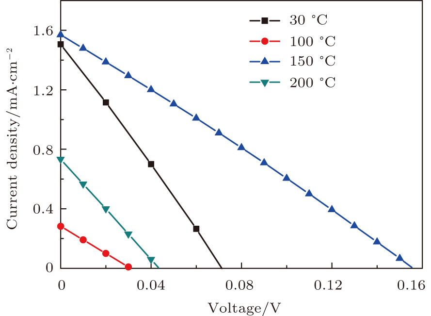 | Fig. 3. (color online) J–V measurements of the solar cells with the buffer layer deposited at different temperatures under AM1.5 solar illumination conditions. |
| Table 4.
Performance characteristics of the solar cells with the buffer layer deposited at 30 (room temperature), 100, 150, and 200 °C, respectively. . |
4. Conclusion
In summary, we have studied the influence of the deposition temperature of the buffer layer on the band alignment of CZTS/In2S3 heterostructures. It is found that the VBO values are 


Reference
| [1] | |
| [2] | |
| [3] | |
| [4] | |
| [5] | |
| [6] | |
| [7] | |
| [8] | |
| [9] | |
| [10] | |
| [11] | |
| [12] | |
| [13] | |
| [14] | |
| [15] | |
| [16] | |
| [17] | |
| [18] |