Enhancement of subgap conductance in a graphene superconductor junction by valley polarization
Li Chuan-Xin1, Wang Sa-Ke2, Wang Jun2, †
College of Mathematics and Physics, Jingchu University of Technology, Jingmen 448000, China
Department of Physics, Southeast University, Nanjing 210096, China


† Corresponding author. E-mail: jwang@seu.edu.cn

Abstract

We theoretically study the differential conductance of a graphene/graphene superconductor junction, where the valley polarization of Dirac electrons is considered in the nonsuperconducting region. It is shown that the subgap conductance will increase monotonically with the valley-polarization strength when the chemical potential µ is near the Dirac point µ ≤ 3Δ (Δ is the superconducting gap), whereas it will decrease monotonically when µ is far away from the Dirac point, µ ≥ 5Δ. The former case is induced by the specular Andreev reflection while the retro-reflection accounts for the later result. Our findings may shed light on the control of conductance of a graphene superconductor junction by valley polarization.

1. Introduction

Since graphene was exploited successfully by Geim and Novoselov a decade ago,[1] a surge of experimental and theoretical research on graphene has been made. The graphene subject will continue to attract much attention of researchers, because many topics of condensed matter physics can be done and extended in the graphene platform[26] due to the material advantages or, more specifically, the linear energy dispersion relation of Dirac electrons in just one-atom-layer thick and honeycomb-like materials.

Recently, valleytronics as a new discipline is increasingly rising and referred to as the electronics based on the valley degree of freedom of electrons in two-dimensional (2D) honeycomb lattice materials such as graphene, silicene, MoS2.[711] Valleytronics concerns the exploitation of the two degenerate but inequivalent Dirac points K, K′ of the Brillouin zone related by the time-reversal symmetry. Several very recent experimental works[1214] have successfully measured the valley currents in the monolayer or bilayer graphene system, and this will further ignite new interest in exploring the valley degree of freedom of Dirac electrons to fabricate quantum devices.

The main challenge in valleytronics is to generate, manipulate, and detect the valley currents; so many works have been dedicated to those three aspects for possible applications in the future valley-based electronic devices.[1518] In our previous works, we have studied using the valley polarization to control the Cooper-pair transport in graphene superconductor systems like realizing a \pi-state Josephson junction or splitting Cooper pair in real space.[19,20] Along the same route, in this work we will continue to study the valley polarization effect on the differential conductance of a graphene/superconductor graphene (G/GS) junction and aim to distinguish the specular Andreev reflection and retro Andreev reflection by using the very different transport properties. The specular Andreev reflection is famous in the graphene system that the reflected hole will not lie in the same band of the impinging electron upon the junction interface.[21] In graphene, this has been proved probable when the chemical potential is near the Dirac point.

Based on a low-energy continuum model and the Dirac Bogoliubov–de-Gennes equation, we found that the subgap conductance of the G/GS junction exhibits very different behaviors, it can either increase or decrease with the valley polarization of Dirac electrons, which depends on the dominant process of the specular or retro Andreev reflection (AR). Therefore, the valley-polarized electrons can be used to distinguish these two AR processes.[21,22]

2. Theoretical model and formalism

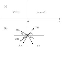
The system under consideration is a uniform graphene in the (x,y) plane, as shown in Fig. 1(a). The region x < 0 is valley-polarized graphene with the combined actions of the off-resonant circularly polarized light field and the static staggered potential kλ + Ez in K, K′ valleys, while x > 0 is covered with a superconducting electrode and finite pairing amplitude Δ is induced, thus the Dirac point is shifted from the Fermi level of the graphene layer via the proximity effect,and the case is abbreviated as “Homo-S”.[19] For convenience, in what follows, we assume λ = E z , and valley polarization strength is 2λ for k = 1 and k = 0 for k = 1.

Fig. 1. (a) A schematic figure of the G/GS junction on graphene. The width of graphene is W and the interface is at x = 0 (top panel). (b) The incident angle of an electron θ e, the normal reflection angle θ e, the Andreev reflection angle θ h, the transparent angle of an elq α e, the transparent angle of a hlq α h. IE, NR, AR, TE, and TH denote the processes of the incident electron, the normal reflection electron, the Andreev reflection hole, the transparent electron-like quasi-particle, and the transparent hole-like quasi-particle, respectively (bottom panel).

In order not to mix with the valley polarization, the spin degree of freedom remains inactive and this simplification leads to a 16×16 matrix degenerating to two 4×4 matrices, which is the Nambu space ∗ pseudospin space of A and B sublattices. In the region x < 0, the two 4×4 matrices degenerate farther to four 2×2 matrices, where only the pseudospin spaces of A and B sublattices couple each other.

The low-energy electron dispersion arbitrarily close to the Dirac points K (k = 1) and K′ (k = −1) of a uniform graphene sheet is given by

(1)
where v is the energy-independent Fermi velocity, and q x , q y are the x component and y component of the momentum measured from Dirac points K and K′ so that |qa| 1 (with a being the lattice constant), and λ,E z are related to the light field strength and the static staggered potential, respectively, and thus +E z represents the combined actions of λ and E z . With λ = 0 or E z = 0, we cannot obtain valley polarization effect at all. In other words, the light field alone or the static staggered potential alone cannot behave as a valley polarizer!

In order to form a Cooper pair, the incident electron (IE) and Andreev reflected hole must be taken from opposite corners K and K′ of the Brillouin zone on a G/GS junction interface, and thus Andreev reflection switches valleys in the graphene sheet.

For an incident electron from Dirac points K and K′, the wavevectors of the incoming electron and the reflected hole are

Further physics analysis shows: (i) when ε < µ − 2λ), the incident electron and the reflected hole are both in the same conduction band, and this is named intraband Andreev reflection or retro-AR; (ii) when µ > ε > µ − 2λ, there exists a forbidden band rather than a dot partitioning two kinds of ARs; (iii) when ε > µ, the reflected hole is an empty state in the valence band in another Dirac point, and this is interband AR or specular-AR.

The differential conductance of the tunnel junction at zero temperature which follows from the Blonder–Tinkham– Klapwijk formula is[23]

(4)
and q is the wavevector of incident electron, while r and r a are normal reflection coefficient and AR coefficient, respectively (see Appendix A). Incident electrons from Dirac points K, K′ are represented by i = +1 and i = 1. The factor 2 is attributed to a two-fold spin degeneracy, while a two-fold valley degeneracy is removed by valley polarization.

For the one-dimensional free and “ultra-relativity” electron, the number of propagating channels of an incident electron in the Dirac point K is

While that in K′ is

The total number of propagating channels of an incident electron is

Thus subgap conductance can be rewritten as

In accordance with Ref. [21] we define

(7)
so we can obtain subgap conductance normalized by G 0
(8)
which is dimensionless. Once g is obtained, it is straightforward to calculate the valley polarizability,[24,25] which is explicit in physics.

3. Results and discussion

There are eight independent parameters in the formula of the valley-polarized conductance g after integrating with respect to the incident angle θ e, which are Δ, µ, ε, U 0, φ, k, λ, and E z . To reduce the number of adjustable parameters, we set E z = λ, and have a combined valley polarization strength 2λ for Dirac point K and 0 for Dirac point K′ (as done in the former description). In the following calculations, we also set φ = 0, Δ = 1, U 0 = 22Δ.[19,21] Here U 0 is a finite value. After these assumptions there are only three independent parameters for the valley-polarized conductance g: ε, µ, and λ.

Let us estimate the amplitude of G 0 from Eq. (7). In realistic graphene tunnel junctions, the amplitude of ∆ would be of the order of 1 K (temperature), we have

(9)
where k B is the Boltzmann constant and T is the temperature. We choose W = 1µm = 10 6 m for a typical mesoscopic size. The constant slope of the dispersion relation \hbar v is of 10 28 J · m, thus WΔ/ \pi\hbar v ~ 100 which is a dimensionless value. While 2e2 /h~10 4 A/V. So the quantum conductance of a GS junction is estimated to be of 10 4 A/V.

We first simply summarize the conductance of G/GS junction in Fig. 2, where the valley polarization strength λ = 0 and the chemical potential µ = 0Δ, 0.2Δ, 0.5Δ, 0.75Δ, 1Δ, 3Δ, and 5Δ, respectively.[21] Since ε and q y are conserved upon ballistic scattering in x < 0 and x > 0 regions, we obtain
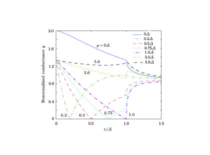
Fig. 2. (color online) Differential conductance versus bias voltage for λ = E z = 0. No valley polarization is considered here.

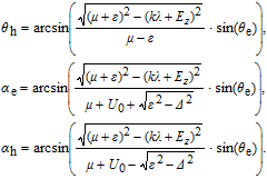
For ε < µ, we have θh > 0 (we assume earlier θ e > 0), then θ h and θ e are on the same side and the Andreev reflected hole is in the conduction band, namely retro-AR, while for ε > µ, due to θ h < 0, θh is on the other side and the hole is in the valence band, namely specular-AR. Thus the normalized subgap conductance

when the valley polarization strength λ = 0. For the case ε < µ, the increase of ε leads to the increase of retro-AR re flected angle θh, which leads to the decrease of subgap conductance for a given chemical potential µ; for ε > µ, the increase of ε leads to the decrease of specular-AR reflected angle θ h, which leads to the increase of subgap conductance g for a given µ; for ε = µ, θ h 90 º leads to the absence of Andreev reflection due to DBdG equation and normal reflection coefficient r = 1, which leads to the normalized subgap conductance g = 0 for any given value of µ. The subgap conductance curve for µ = 0Δ is always the specular-Andreev reflection, but those cases for µ = 1.0Δ, 3.0Δ, and 5.0Δ are always retro-Andreev reflection (retro-AR). The subgap conductance curves for µ = 0.2Δ, 0.5Δ, and 0.75Δ have retro-AR and specular-AR simultaneously in a given chemical potential µ, and all three curves have a bending structure at ε = µ, where a dot separates retro-AR and specular-AR. For a normal metalsuperconduction junction, we always have ε < µ, strictly satisfying the relation θh = θe, which is a truly retro-AR process, that is, the trajectories of the Andreev-reflected holes retrace the trajectories of the incident electrons. As a matter of fact, most of the Andreev reflections studied in literature are retro-AR, until the discovery of graphene in 2004, which has a smaller chemical potential µ, and Beenakker first discussed the superconducting graphene junction and specular-AR in 2006.[21]

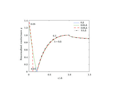
Secondly, we focus on the subgap conductance for µ = 0.2Δ in Fig. 3 where λ = 0Δ, 0.01Δ, 0.05Δ, and 0.1Δ. First, the four line shapes of subgap conductance can be understood by the following argument. For the case µ = 0.2Δ, we have

As for case λ = 0Δ, the retro-AR dominates the process when ε < 0.2Δ, while the specular-AR dominates the reflection when ε > 0.2Δ. There is no valley polarization where the two kinds of Andreev reflection are separated by just a dot ε = µ = 0.2Δ. When µ = 0.2Δ and λ = 0.01Δ, the whole curve can be divided into 3 segments: i) For ε < 0.18Δ, we have the Andreev reflected angle θh > 0; ii) For 0.18Δ < ε < 0.2Δ, the wave number qh2 becomes an imaginary number and this kind of wave cannot spread across the valley polarization

The increase of λ leads to the decrease of the channel’s number factor N and the increase of the integrating factor via the decrease of the Andreev reflected angle θ h, but the comprehensive effect of the increase of λ is the increase of the normalized subgap conductance g for the case µ = 0.2Δ. Regardless of whether the left-hand member and the right-hand member of any forbidden band in Fig. 3, the subgap conductance increases with increasing the valley polarization strength λ.

Fig. 3. (color online) Subgap conductance spectra for µ = 0.2Δ in the G/GS junction.

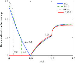
As for µ = 0.5Δ, there exist four curves for λ = 0Δ, 0.1Δ, 0.2Δ, and 0.25Δ in Fig. 4. There are lots of similarities between Fig. 3 and Fig. 4, but longer forbidden band widths and greater increase of subgap conduction due to the graphene; iii) For ε > 0.2Δ, we have θ h < 0. Thus, the case for λ = 0.01Δ has a forbidden band width from ε = 0.18Δ to ε = 0.2Δ, while the region ε < 0.18Δ is for retro-AR and the interval 1.0Δ > ε > 0.2Δ for specular-AR. When λ = 0.05Δ, the region 0.1Δ < ε < 0.2Δ is forbidden band width, and the regions on the left and the right are retro-AR and specular segments, respectively. In particular, the retro-AR disappears when valley polarization strength λ = 0.1Δ, and this leads to the fact that all the region ε < 0.2Δ is the forbidden band width, the region ε > 0.2Δ is for specular-AR. What separates retro-AR and specular-AR is a forbidden band width (no longer just a dot) for valley polarization strength λ ≠ 0Δ as shown in Fig. 3. Below is a summary of which subgap conductance varies when λ varies for a given µ. For this case, we have increasing valley polarization strength in Fig. 4. Here when λ = 0.25Δ, retro-AR disappears.

Fig. 4. (color online) Subgap conductance spectra for µ = 0.5Δ in the G/GS junction.

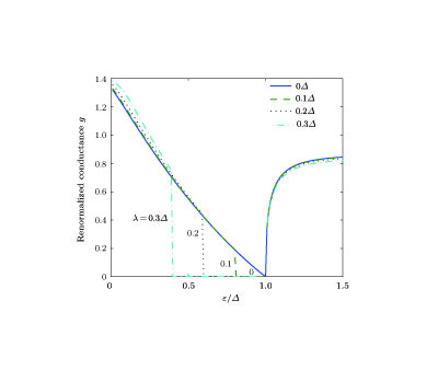
Fourthly, we analyze Fig. 5 for µ = 1Δ. There are four curves for λ = 0Δ, 0.1Δ, 0.2Δ, and 0.3Δ, respectively. These curves of the conductance spectra show a linear relation approximately, and the subgap conductance g decreases with the increase of the incident electron energy ε for all the curves in Fig. 5. At λ = 0Δ, having no valley polarization, conductance equals to zero value at the dot ε = µ = 1Δ, while the other three curves are different from the case of λ = 0Δ and have fi-nite forbidden band width. The cases for λ = 0.1Δ, 0.2Δ, and 0.3Δ have forbidden band widths from ε = 0.8Δ to 1Δ), 0.6Δ to 1Δ and 0.4Δ to 1Δ, respectively. As seen in Fig. 5, the sub-gap conductance increases with the increase of valley polarization strength λ. To better understand these findings, let us come into concrete analysis. For the region 0.6Δ < ε < 0.8Δ, there are only two curves: λ = 0Δ and λ = 0.1Δ, and we can distinguish subgap conductance for λ = 0.1Δ is greater than that for λ = 0Δ through a magnifying lens in the menu of software MATLAB. Likewise,three curves for the region 0.4Δ < ε < 0.6Δ and four curves for region ε < 0.4Δ are the same as they were before.

Fig. 5. (color online) Subgap conductance spectra for µ = 1.0Δ in the G/GS junction.

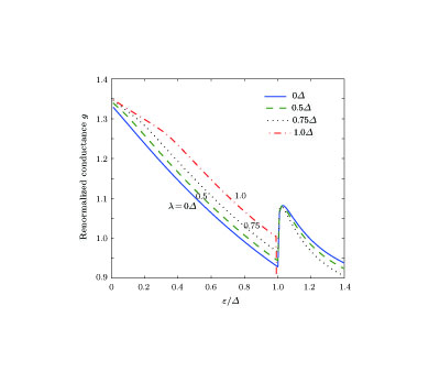
In Fig. 6, we show the case of µ = 3Δ for λ = 0Δ, 0.5Δ, 0.75Δ, and 1.0Δ, respectively. The specular AR disappears but the retro AR dominates in those four curves throughout all subgap segment. Obviously, the subgap conductance monotonically becomes larger when the valley polarization strength λ increases.

Fig. 6. (color online) Subgap conductance spectra for µ = 3.0Δ in the G/GS junction.

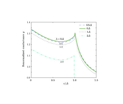
Finally, we want to emphasize the case of µ = 5Δ in Fig. 7. Similar to Fig. 5 and Fig. 6, there are no specular- AR throughout the subgap segment. When the valley polarization strength λ = 2Δ, the region ε > 1Δ is the forbidden band which the other curves for λ = 0Δ, 0.5Δ, and 1.0Δ have not. Above all, subgap conductance decreases with the increase of valley polarization strength λ for the case µ = 5Δ. This case is completely contrary to those cases for µ = 0.2Δ, 0.5Δ, 1.0Δ, and 3Δ in Figs. 3, 4, 5, and 6. For the case µ = 5Δ, the change of valley polarization strength λ leads to the change of the channel’s number factor N and the integrating factor, but the final effect is the decrease of the normalization subgap conductance g with the increase of valley polarization strength λ. Further study shows the same changing trends of subgap conductance for µ > 5Δ as that for µ = 5Δ.

Fig. 7. (color online) Subgap conductance spectra for µ = 5.0Δ in the G/GS junction.

From the above discussion, we can make some concrete conclusions. At µ = 0, it is impossible that graphene is valleypolarized for this parabola-like dispersion relation, and there exists only specular-AR for all ε value. There are retro-AR and specular-AR for µ = 0.2Δ and µ = 0.5Δ), but only retro-AR survives at µ = 1.0Δ, µ = 3Δ, and µ = 5Δ. No specular-AR exists for µ > 1.0Δ. The theoretical calculations also show the subgap conductance increases with an increase of valley polarization strength for µ = 0.2Δ, 0.5Δ, 1.0Δ, and 3Δ, but decreases at µ = 5Δ. In particular, for the cases µ = 0.2Δ and µ = 0.5Δ, which simultaneously possess retro-AR and specular-AR, their subgap conductances have a common variation trend. Of course, the forbidden band conductance keeps zero invariably. The reason is as follows. The increase of valley polarization strength λ leads to the decrease of the AR angle θ h, which leads to the increase of the subap conductance; while the increase of λ responds to the decrease of the number of propagating channels N, which causes in turn the decrease of the subgap conductance. The practical variation of subap conductance depends on the competition of the two factors, θ h and N.

4. Conclusion

In summary, we have demonstrated theoretically that the differential conductance of the G/GS junction can be affected by the valley polarization, which is coming from the combined actions of the static staggered potential E z and the off-resonant circularly polarized light field strength λ. The subgap conductance of the G/GS junction decreases monotonously with an increase of valley polarization when the retro-AR is dominant. In contrast, the conductance will increase significantly with the valley polarization when the chemical potential µ 3Δ and the specular-AR mainly contributes to the conductance.

(A1)
where σ 0 is a 2 × 2 unit matrix, σ i for i = 1,2 is the Pauli matrix representing the pseudo-spin space of A, B sublattices, and p i for i = 1,2 is the momentum. The block-diagonalized matrix has eigenvalues
(A2)
where the wavevector q = (q x ,q y ), ε k is the excitation energy of Dirac points K and K' , respectively. Upon ballistic scattering, particle energy ε and transverse wavevector q y are conversed. The transverse wavevector of an electron is given by
(A3)
and that of a hole is
(A4)
Equation (A2) has four eigenvectors. For a right-moving electron at angle of incident θ e, the eigenvector reads
(A5)
while that of a left-moving electron reads
(A6)

For a right-moving hole with an incident angle qh, the eigenvector reads

(A7)
while that of a left-moving hole reads
(A8)

In Fig. 1(b), we assume an electron incidence for the conductance computation of the GS junction without loss of generality, where there are only three eigenvectors (right-moving hole for an electron incident θ h does not exist).

Our findings demonstrated that the valley polarization can be used to distinguish the specular-AR from the retro-AR process in the G/GS junction.

Appendix: The calculation of Andreev reflection angle, coefficient, and normal reflection coefficient
A1. Scattering states in region x < 0

For the region x < 0, electron and hole excitations are decoupled and described by the Dirac equation

A2. Scattering states in region x > 0

For region x > 0, electron and hole excitations are coupled together by the superconducting pair potential Δ and described by the DBdG equation (Dirac–Bogoliubov–de Gennes)

(A9)
where the amplitude Δ and the phase φ are the order parameters of the pair potential, which couples time-reversal electron and hole states and produces the coupled Nambu space. Equation (A9) has eigenvalues
(A10)
Thus,the transverse wavevector of an electron is
(A11)
while that of a hole is
(A12)

For a right-moving electron-like quasi-particle (elq) at angle of transparent α e, the eigenvector reads

(A13)
while for a left-moving elq with angle α e, we have eigenvector
(A14)

For a right-moving hole-like quasi-particle (hlq) at the angle α h, the eigenvector reads

(A15)
while for a left-moving hlq at angle α h, the eigenvector reads
(A16)

In this letter, we just use the eigenvectors of a right-moving elq and a right-moving hlq in the circumstance Fig. 1(b).

A3. Interface in x = 0

For an incident electron with angle θ e in Fig. 1(b), there are four physical phenomena: normal reflection with angle θ e, Andreev reflection with angle θ h (retro-Andreev reflection for µ > ε, and specular-Andreev reflection for µ < ε), transparent elq with angle αe and transparent hlq with angle αh. Owing to the ballistic scattering at the interface, ε and qy are conserved in regions x < 0 and x > 0, we obtain

that is
(A17)

Because Dirac equation and DBdG equation are all differential equation of the first order, we only apply the continuity condition at the interface x = 0

(A18)
where r a is the Andreev reflection coefficient and r is the normal reflection coefficient, while t e and t h are elq and hlq transparent coefficients, respectively. Equation (A18) is an actual equations set, which combines with Eqs. (A5), (A6), (A8), (A13), and (A15), and we can obtain the corresponding four coefficients r a, r, t e, and t h.

Only the Andreev reflection angle θ h, Andreev reflection coefficient r a, and normal reflection coefficient r were quoted in the main text of this paper.

Reference
[1] Novoselov K S Geim A K Morozov S V Jiang D Zhang Y Dubonos S V Grigorieva I V Firsov A A 2004 Science 306 666
[2] Sun L F Fang C Liang T X 2013 Chin. Phys. B 23 047201
[3] L C Pereira P A Schulz 2008 Phys. Rev. B 77 075416
[4] Deng W Y Zhu R Xiao Y C Deng W J 2014 Chin. Phys. B 23 017202
[5] Yokoyama T Linder J Sudbo A 2008 Phys. Rev. B 77 132503
[6] G Tkachov 2009 Phys. Rev. B 79 045429
[7] Wang S K Tian H Y Yang Y H Wang J 2014 Chin. Phys. B 23 017203
[8] Ezawa M 2012 Phys. Rev. Lett. 109 055502
[9] Ezawa M 2013 Phys. Rev. Lett. 110 026603
[10] Guo H H Yang T Tao P Zhang Z D 2014 Chin. Phys. B 23 017201
[11] Kioseglou G Hanbicki A T Currie M Friedman A L Gunlycke D Jonker B T 2012 Appl. Phys. Lett. 101 221907
[12] Huard B Scupizio J A Stander N Todd K Goldhaber-Gordon D 2007 Phys. Rev. Lett. 98 236803
[13] Stander N Huard B Goldhaber-Gordon D 2009 Phys. Rev. Lett. 102 026807
[14] Heersche H B Jarillo-Herrero P Oestinga J B Vandersypen L M K Morpurgo A F 2007 Eur. Phys. J. 148 27
[15] Tikhonenko F V Horsell D W Gorbachev R V Savchenko A k 2008 Phys. Rev. Lett. 100 056802
[16] Heersche H B Jarillo-Herrero P Oostinga J B Vandersypen L M K Morpurgo A F 2007 Nature 446 56
[17] Rycerz A Tworzydlo J Beenakker C W J 2006 arXiv: condmat/0608533v2 [cond-mat. mes-hall]
[18] Feng Z 2012 Phys. Rev. B 85 155415
[19] Wang J Yang Y H Chan K S 2014 Phys. Rev. B 89 064501
[20] Wang J Hao L Liu J F 2016 Phys. Rev. B 93 155405
[21] Beenakker C W J 2006 Phys. Rev. Lett. 97 067007
[22] Asano Y Yoshida T Tanaka Y Golubov A A 2008 Phys. Rev. B 78 014514
[23] Blonder G E Tinkham M Klapwijk T M 1982 Phys. Rev. B 25 4515
[24] Takashina K Niida Y Renard V T Piot B A Tregurtha S D Fujiwara A Hirayama Y 2013 Phys. Rev. B 88 201301
[25] Akhmerov A R Beenakker C W J 2007 Phys. Rev. Lett. 98 157003