Enhancement of subgap conductance in a graphene superconductor junction by valley polarization
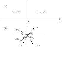
(a) A schematic figure of the G/GS junction on graphene. The width of graphene is W and the interface is at x = 0 (top panel). (b) The incident angle of an electron θ e, the normal reflection angle θ e, the Andreev reflection angle θ h, the transparent angle of an elq α e, the transparent angle of a hlq α h. IE, NR, AR, TE, and TH denote the processes of the incident electron, the normal reflection electron, the Andreev reflection hole, the transparent electron-like quasi-particle, and the transparent hole-like quasi-particle, respectively (bottom panel).