Room temperature NO2-sensing properties of hexagonal tungsten oxide nanorods
Wu Yaqiao1, 2, Hu Ming1, †, Tian Yuming2
School of Electronics and Information Engineering, Tianjin University, Tianjin 300072, China
Taiyuan University of Science and Technology, Taiyuan 030024, China


† Corresponding author. E-mail: huming@tju.edu.cn

Project supported by the National Natural Science Foundation of China (Grant Nos. 60771019, 61271070, and 61274074) and the Tianjin Key Research Program of Application Foundation and Advanced Technology, China (Grant No. 11JCZDJC15300).

Abstract

Hexagonal WO3 nanorods were synthesized through a facile hydrothermal method. The nanorods properties were investigated by scanning electron microscope (SEM), transmission electron microscope (TEM), energy dispersive spectroscopy (EDS), and x-ray diffraction (XRD). The NO2-sensing performances in terms of sensor response, response/recovery times and repeatability at room temperature were optimized by varying the heat treatment temperature of WO3 nanorods. The optimized NO2 sensor (400-°C-annealed WO3 nanorods) showed an ultra-high sensor response of 3.2 and short response time of 1 s to 5-ppm NO2. In addition, the 400-°C-annealed sample exhibited more stable repeatability. Furthermore, dynamic responses measurements of annealed samples showed that all the annealed WO3 nanorods sensors presented p-type behaviors. We suppose the p-type behavior of the WO3 nanorods sensor to be that an inversion layer is formed in the space charge layer when the sensor is exposed to NO2 at room temperature.Therefore, the 400-°C-annealed WO3 nanorods sensor is one of the most energy conservation candidates to detect NO2 at room temperature.

1. Introduction

According to the EPA (United States Environmental Protection Agency), NO2 is used as the indicator for the larger group of nitrogen oxides. NO2 is the main source in the production of ground-level ozone and fine particle pollution except for contributing to the formation of acid rain and smog. Therefore, in January 2010, EPA established an additional primary standard for NO2 at 100 ppb, averaged over one hour. In order to detect NO2, many researchers have reported nanostructure metal oxide based NO2 sensors.[18] These gas sensors usually were operated at the temperature range of 100 °C–300 °C resulting in high electrical power consumption, which limited the use of the metal oxide based sensor as a sensing element in battery-powered portable devices.[9] Among various nanostructure metal oxide semiconductor materials, tungsten oxide nanorods/nanowires, which can achieve a low operation temperature since WO3 has a lower integrating energy barrier than SnO2 or TiO2,[1016] are highly promising candidates for detecting NO2. Therefore, it is prospective to develop a low-cost, low power consumption, high-sensitivity and stable NO2 gas sensor based on tungsten oxide nanorods/nanowires.

In most cases, sensing films were prepared by wet chemical methods, so the process of thermal treatment is a necessary step, which not only can burn out the organic solvent used in preparation of coating slurry but also can enhance the adherence between the sensing film and the sensor substrates. More importantly, thermal treatment could stabilize the sensing film's microstructure and then improve the reliability and stability of the gas sensor.[17] However, the gas sensing material would gradually undergo a series of morphological evolutions and obvious changes of phase composition with the increase of temperature. On the other hand, these changes are the main factors which would influence the gas-sensing properties of oxide semiconductor based sensors.[18] Therefore, it is significant to comprehensively understand the relationship between the annealing-induced microstructure changes and the gas-sensing properties of the one-dimensional tungsten oxide.

Next, metal oxides based gas sensors are classified as n-type or p-type according to whether they show a decrease or an increase of conductivity when they are exposed to an oxidizing gas (such as NO2).[19,20] WO3 nanorods sensors which were operated at high temperature are known to behave as an n-type semiconductor.[2125] The p-type semiconductor based on WO3 nanorods operating at room temperature is rarely reported. Consequently, this paper is focused on the sensing property of WO3 nanorods sensor at room temperature.

In this study, WO3 nanorods are prepared by a facile hydrothermal method and the relationship is investigated between the microstructures and gas sensing properties of WO3 nanorods sensors annealed at 300, 400, and 500 °C, respectively. In addition, the p-type semiconductor gas sensing mechanism of the WO3 nanorods sensor is discussed.

2. Experimental section
2.1. Synthesis of WO3 nanorods

WO3 nanorods were synthesized through hydrothermal technology. In a typical procedure, 0.01-mol Na2WO4·2H2O and 0.02-mol NaCl were dissolved in 60-ml deionized water and stirred for 30 min by magnetic stirring apparatus. Na2WO4·2H2O was served as a precursor and NaCl was used as structure directing agents (SDAs) which have been proven to facilitate the controllable growth of nanostructure WO3. The pH value of the solution was fixed at 2.5 which was adjusted by using 3-M HCl solution. Then, the obtained uniform mixture was transferred into a 100-ml Teflon-lined stainless steel autoclave and heated at 180 °C for 24 h in an electric oven. After naturally cooling down to room temperature, the resultant precipitates were washed with deionized water and ethanol by a centrifuger several times and dried in a vacuum at 80 °C for 10 h. Finally, the slurry of as-prepared tungsten oxide nanorods was prepared by ultrasonically mixing tungsten oxide nanorods and terpineol, which acted as a vehicle binder and solvent. In this experiment, all reagents were purchased from the Guangfu Fine Chemical Research Institute (Tianjin, China).

2.2. Sensor fabrication and NO2 response measurement

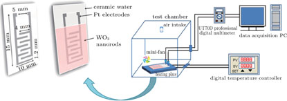
Firstly, a pair of interdigital Pt electrodes was deposited on the cleaned alumina substrates by RF magnetron sputtering using a shadow mask. In detail, the DPS–III ultrahigh vacuum facing-target magnetron sputtering system was used to deposit Pt electrical contacts and operating parameters were listed as follows: the RF power was 90 W, the base vacuum pressure was 4.0 × 10⁻⁴ Pa and the working pressure was 2 Pa. Secondly, the coating slurry was prepared by mixing the nanorods (30 mg) in terpineol (0.2 ml) and then ground in an agate mortar for 30 min to obtain a homogeneous paste. The resulting paste was coated on those alumina substrates by the spin-coating method. Thirdly, the WO3 nanorods sensors were annealed at 300, 400, and 500 °C for 2 h in the air with a heating rate of 6 °C/min, respectively. Then the gas-sensing characteristics of as-prepared sensors were tested in a computer-controlled static gas sensing characterization system which consists of a 30-L sealed organic glass test chamber, a professional digital multi-meter, a data acquisition system and a flat heating plate with an adjustment range from room temperature (RT) to 300 °C.[26] The programmable multi-meter was connected to the data acquisition system, which was used for continuously recording the resistance changes of the sensor and the sampling interval was set to 1 s. The schematic diagram of the sensor and the measurement system are depicted in Fig. 1. When exposed to NO2, the sensor response presented a p-type feature at room temperature. Hence, the response is defined as S=Ra/Rg, where Ra and Rg are the resistances of the sensor element in the presence of atmospheric air and target gas respectively. The time taken by the sensor to achieve 90% of the total resistance change is defined as the response and recovery time.

Fig. 1. (color online) The schematic diagram of the sensor and the measurement system.
2.3. Characterization of WO3 nanorods

The morphology, element composition and crystal structure of the WO3 nanorods were characterized using a field emission scanning electron microscope (FESEM, FEI Nanosem 430), energy dispersive spectroscopy (EDS) attached on the FESEM, transmission electron microscope (TEM, TECNAIG2F-20) and x-ray diffraction (XRD, RIGAKU D/MAX 2500V/PC, Cu Kα radiation).

3. Results and discussion
3.1. Effects of annealing on microstructure

Typical FESEM image of as-synthesized WO3 nanorods is shown in Fig. 2(a), from which we can see that those nanorods exhibit a one dimension structure with lengths in the range of 3 μm–5 μm and cross sections in the range of 50 nm–150 nm. Nevertheless, there still exist nanorod bundles which are induced by larger surface areas and their intrinsic defects such as shear planes, oxygen vacancies, and stacking faults.[27,28] Further characterizations of the morphology and crystallinity of the WO3 nanorods were investigated by TEM and high resolution transmission electron microscope (HRTEM) as shown in Fig. 2(b) and Fig. 2(c). It can be seen that the lattice fringe separation is about 0.323 nm, corresponding to the lattice space of the hexagonal WO3 (200) plane. In order to investigate the morphology evolution of WO3 nanorods with increasing annealing temperature, the SEM images of annealed WO3 nanorods coated on ceramic wafer by spin coating are illustrated in Fig. 3. The appearance of annealed nanorods is changed pronouncedly compared with that of raw WO3 nanorods (Fig. 2(a)). After being processed at 300 °C for 2 h, the diameter of all the nanorods is still in the range of 50 nm–150 nm but the lengths reduce sharply through a fracture of nanorods (Fig. 3(a)). The morphology feature remains stable after annealing at 400 °C (Fig. 3(b)). When increasing the temperature to 500 °C, it is apparent that the morphological characteristic of the nanorods almost disappears completely, and nanoparticles which display pronounced facet structures with polygonal cross-sections are formed instead, indicating that a possible agglomeration occurs (Fig. 3(c)).

Fig. 2. (color online) SEM, TEM, and HRTEM images of WO3 nanorods.
Fig. 3. SEM images of WO3 nanorods after (a) 300-°C, (b) 400-°C, and (c) 500-°C thermal treatment.

The surface morphology of the square-marked area and the corresponding EDS spectrum of WO3 nanorods with annealed samples are shown in Fig. 4. Every EDS spectrum contains the characteristic peaks of C, O, Na, and W, and all the annealed sensors still include the characteristic peaks of Al and Pt. The elements concentration of (a) the pristine WO3 nanorods together with (b) 300-°C-annealed, (c) 400-°C-annealed, and (d) 500-°C-annealed sensor are illustrated in Table 1.
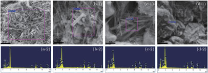
Fig. 4. (color online) The surface morphology of selected area and corresponding EDS spectrum of (a) WO3 nanorods, (b) 300-°C-, (c) 400-°C-, and (d) 500-°C-annealed samples.
Tab1e 1. The elements concentration of (a) the pristine WO<sub>3</sub> nanorods together with (b) 300-°C-annealed, (c) 400-°C-annealed, and (d) 500-°C-annealed sensor. .

The elements concentration of (a) the pristine WO3 nanorods together with (b) 300-°C-annealed, (c) 400-°C-annealed, and (d) 500-°C-annealed sensor are illustrated in Table 1. The sum of the weight concentrations is equal to 100%.The atomic ratio of W and O should be 1:3 as a result of the chemical reaction, but their measuring value of atomic ratio calculated by EDS quantitative analysis software is (a) 1:4, (b) 1:5, (c) 1:5, and (d) 1:7. We surmised the additional O atomic of the pristine WO3 nanorods and 500-°C-annealed samples may come from adsorbed oxygen and NaO which is the residual decomposition product of Na2WO4·2H2O. Besides the above three O elements supplies, a portion of O elements come from Al2O3 substrate owing to that we have detected an Al element in the 300-°C- and 400-°C-annealed samples. The Pt elements in the EDS may come from the alumina substrates deposited with a pair of interdigital Pt electrodes. This can be certified by the result of XRD analysis. The appearance of the C element can be attributed to the SEM grid.

In order to estimate O elements weight% derived from adsorbed oxygen, we have calculated the O elements weight% derived from other oxide. For example, the relative molar mass of W and O in the WO3 molecule is 184:48. The weight% of W elements is 70.39% in the pristine WO3 nanorods, so the weight% of O elements in WO3 is 18.36%.The results are shown in Table 2.

Tab1e 2. The weight% of O elements of (a) the pristine WO<sub>3</sub> nanorods together with (b) 300-°C-annealed, (c) 400-°C-annealed, and (d) 500-°C-annealed sensor. .

On the basis of Table 2, we further estimated the weight% of adsorbed oxygen/μm2 of (a) the pristine WO3 nanorods together with (b) 300-°C-annealed, (c) 400-°C-annealed, and (d) 500-°C-annealed sensor. The results are shown in Table 3. The weight% of adsorbed oxygen/μm2 increased by the way of heat treatment. Considering the sample room of EDS or SEM is pumped into a vacuum state before scanning, the adsorbing power between oxygen and WO3 nanorods should be a chemical bond instead of a physical bond. The chemical bond contains an electrovalent bond and a covalent bond, which were produced by lots of oxygen vacancies. Thus, we consider the oxygen vacancies increased in the nanorods by the way of heat treatment, which can be further confirmed by the XRD.

Tab1e 3. The weight% of adsorbed oxygen/μm<sup>2</sup> of (a) the pristine WO<sub>3</sub> nanorods together with (b) 300-°C-annealed, (c) 400-°C-annealed, and (d) 500-°C-annealed sensor. .

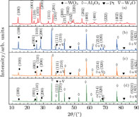
The crystalline phases of WO3 nanorods annealed at different temperatures together with the pristine WO3 nanorods were analyzed by x-ray diffraction. The XRD patterns of the original WO3 nanorods match well with JCPDS NO. 33-1387 for hexagonal WO3 as indicated in Fig. 5(a). In order to avoid the WO3 nanorods being polluted, we directly take the prepared sensors as a test specimen for XRD analysis. Therefore, the main crystalline phases of annealed ones are Al2O3 (JCPDS NO. 46-1212) and Pt (JCPDS NO. 87-0646) except hexagonal WO3 (JCPDS NO. 75-2187). However, it is noteworthy that a new crystalline phase of cubic W3O (JCPDS NO. 02-1138) present in annealed samples as shown in Figs. 5(b), 5(c), 5(d). Its three characteristic peaks which are the (210) peak with I=100 (2θ=40.040), the (320) peak with I=60 (2θ=66.761), and the (421) peak with I=70 (2θ=88.895) match together the Pt (111) peak with I=100 (2θ=39.796), the Al2O3 (214) peak with I=23 (2θ=66.519), and the Al2O3 (0210) peak with I=9 (2θ=88.994). W3O is a kind of metastable and non-stoichiometry tungsten oxide, which has a large number of oxygen vacancies. As the temperature is increased to 500 °C, the characteristic peak of Pt (2θ=67.859) also appears. This is a result of the high annealing temperature making the Pt electrodes be exposed to the outside.

Fig. 5. (color online) XRD patterns of (a) freshly-obtained WO3 nanorods, (b) 300-°C-, (c) 400-°C-, and (d) 500-°C-annealing WO3 nanorods.
3.2. Effects of annealing on gas-sensing properties

We have examined the 300-°C annealed sample by sensing 1-ppm NO2 from room temperature to 250 °C and the sensor showed two completely different sensing behaviors. The WO3 nanorods sensor showed a p-type response at the range of 25 °C–50 °C while an n-type response at the range of 50 °C–250 °C. This work has been published in Ref. [29]. The p-type semiconductor based on WO3 nanorods operating at room temperature is rarely reported. Consequently, this paper is focused on the sensing property of WO3 nanorods sensor at room temperature.

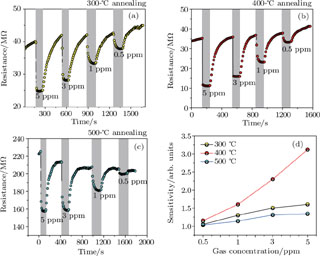
Figure 6 depicts the dynamic responses of the gas sensors based on the WO3 nanorods annealed at (a) 300 °C, (b) 400 °C, and (c) 500 °C to varying NO2 concentration at room temperature (RT). Figure 7 illustrates the relationship between (a) the response time, (b) the recovery time and NO2 concentration for the sensors based on annealed WO3 nanorods at RT. As shown in Figs. 6(a)6(c) and Fig. 7(a), the WO3 nanorods sensors are highly sensitive to NO2 for the resistance of all the sensors decrease abruptly for the NO2 injection period (shadow areas) and can approach the steady-state values within 75 s. In particular, the response time of the 400-°C-annealed sample reduce to 1 s when the sample is exposed to NO2 gas with a concentration of either 3 ppm or 5 ppm. As shown in Figs. 6(a)6(c) and Fig. 7(b), after the removal of NO2, the resistance of all the annealed WO3 nanorods sensors increases and is able to recover to the original value within 200 s. The recovery time reduces to 97 s for 3-ppm NO2 and 152 s for 5-ppm NO2, respectively. Figure 6(d) illustrates the response of the sensors based on annealed WO3 nanorods to varying NO2 concentration at RT. The variation trend of all annealed WO3 nanorods sensors is similar in that the response increases apparently with increasing NO2 concentration. In the case of the 400-°C-annealed sample, there is an obvious increase in the response, with the maximum responses of about 1.3 ppm to 0.5 ppm, 1.7 ppm to 1 ppm, 2.3 ppm to 3 ppm and 3.2 ppm to 5 ppm NO2, respectively. When the heat treatment temperature is increased to 500 °C, the gas sensing property suddenly gets worse. The maximum response is 1.5, when even exposing to 5 ppm. In addition, there is only a slight enhancement in response with increasing NO2 concentration. We assume that the deteriorated sensing properties probably are related with the reduced specific surface areas (Fig. 3(c)). Excepting the recovery time of 500-°C-annealed sensor is shorter than 400-°C-annealed sensor to 5 ppm NO2, in every NO2 concentration, the response time and the recovery time of the 400-°C-annealed sample (red column) is shorter than the 300-°C-annealed sample (yellow column) and the 500-°C-annealed sample (blue column) as shown in Fig. 8.
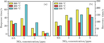
Fig. 6. (color online) Dynamic responses of the gas sensors based on the WO3 nanorods annealed at (a) 300 °C, (b) 400 °C, and (c) 500 °C to varying NO2 concentration at room temperature. (d) Relationship between the responses and NO2 concentration for the sensors based on annealed tungsten WO3 nanorods at room temperature.
Fig. 7. (color online) Relationship between (a) the response time (b) recovery time and NO2 concentration for the sensors based on annealed tungsten WO3 nanorods at room temperature.
Fig. 8. (color online) Schematic energy-level diagram of (a) n-type semiconductor, (b) the formation of depletion layer, (c) the formation of inversion layer.

In a word, from Fig. 6 and Fig. 7 we can see that the 400-°C-annealed sample has more excellent sensing performance at room temperature compared with both 300-°C- and 500-°C-annealed WO3 nanorods sensors. We suppose that the excellent gas sensing properties of the 400-°C-annealed sample could be attributed to its moderate crystallinity, larger specific surface areas and more oxygen vacancies. Therefore, the excellent gas sensing properties of hydrothermal-prepared WO3 nanorods make it an ideal candidate for detecting NO2 at room temperature.

3.3. Gas-sensing mechanism

When operated at high temperature, tungsten oxide sensors are known to behave as n-type semiconductors. One of the conceivable mechanisms for the p-type conductive behavior at RT is the formation of an inversion layer on the surface of WO3 nanorods. Owing to the fact that bulk defects equilibrate quite slowly at RT, surface conduction is dominant. The surface of the semiconductor is composed of a surface layer and space charge layer. Because of the existence of large density of surface states which mainly was induced by dangling, structural defects and gas adsorption, too many charges accumulated on the surface layer, which led to an aggregation layer, depletion layer, or even inversion space-charge layer below the surface layer of the semiconductor as shown in Fig. 8. In the energy-level diagram of the n-type semiconductor, the Fermi level approaches the bottom of the conduction band and above the intrinsic level, as shown in Fig. 8(a). When the WO3 nanorods sensors are exposed to air, oxygen molecules are absorbed on the surface of WO3 nanorods and form chemisorbed oxygen species by capturing electrons from the conduction band of WO3 nanorods (Eqs. (1) and (2)). Then the energy level of WO3 nanorods is upswept and the depletion layer is formed, as shown in Fig. 8(b). When the WO3 nanorods sensors are exposed to NO2, as a powerful oxidizing gas with strong electron-withdrawing power, NO2 is capable of competitively capturing electrons not only from the conduction band of WO3 nanorods but also from chemisorbed oxygen species (Eqs. (3)–(5)). Besides the high surface areas that make the surface more actively adsorb O2 or NO2, there exists a non-stoichiometry monoclinic W3O which has a large amount of oxygen vacancies. It easily adsorbs O2 or NO2 to stabilization.[30] Then with the continuous accumulation of negative charges, too many negative charges aggregate in the surface layer and the inversion layer in which holes become the main charge carrier is gradually generated, as shown in Fig. 8(c). In the energy-level diagram, the Fermi level appears below intrinsic level.

3.4. Repeatability

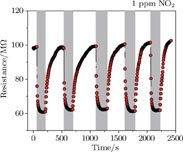
For practical use, the repeatability of the gas sensors is also an important quality factor. Reversible and reproducible responses of the 400-°C-annealed gas sensor upon periodic exposure to NO2 gas of 1 ppm are presented in Fig. 9 with five switching on/off cycles. Notably, the sensor shows a similar response value and response–recovery time, which suggest an excellent repeatability and stability. It is well known that the high crystallinity of the WO3 nanorods is responsible for the high stability of the sensor.[31]

Fig. 9. (color online) Electrical resistance changes of the sensor based on 400-°C annealed WO3 nanorods as a function of time for five cycles at room temperature with 1 ppm of NO2.
4. Conclusions

In summary, WO3 nanorods were successfully synthesized through the hydrothermal method. The microstructures and crystalline phases of both pristine and annealed WO3 nanorods were investigated by SEM, EDS, HRTEM, and XRD. The test results showed that a fracture occurred during annealing treatment. The 300-°C- and 400-°C-annealed samples became shorter than the original WO3 nanorods but the 500-°C-annealed nanorods were shaped into nanoparticles. At the same time the XRD patterns indicated that a new crystalline phase W3O came into being during the thermal treatment process. Moreover, the appearance of a low oxidized tungsten phase W3O was beneficial to the enhancement of the gas sensing performance of WO3 nanorods. Response measurements of annealed samples performed at RT showed that all the annealed WO3 nanorods sensors presented p-type behaviors. We suppose the transition mechanism from n to p-type to be that an inversion layer formed in the space charge layer when the sensors were exposed to NO2 at room temperature. Compared with the 300-°C- and 500-°C-annealed samples, the 400-°C-annealed sample has higher response, quicker response/recovery speed, and more stable repeatability. The excellent gas sensing properties can be attributed to its moderate crystallinity, larger specific surface areas and more oxygen vacancy. This result is important for the future research and development of a gas sensor based on hexagonal WO3 nanorods, which favors low power consumption, high sensitivity and integration technology.

Reference
[1] Afzal A Cioffi N Sabbatini L Torsi L 2012 Sens. Actuators B 171 25
[2] Heidari E K Zamani C Marzbanrad E Raissi B Nazarpour S 2010 Sens. Actuators B 146 165
[3] Lee Y L Tsai W C Chang C H Yang Y M 2001 Appl. Surf. Sci. 172 191
[4] Lee J H Kim J Seo H W Song J W Lee E S Won M Han C S 2008 Sens. Actuators B 129 628
[5] Kim B G Lim D G Park J H Choi Y J Park J G 2011 Appl. Surf. Sci. 257 4715
[6] Karthigeyan A Gupta R P Scharnagl K Burgmair M Zimmer M Sharma S K Eisele I 2001 Sens. Actuators B 78 69
[7] Kunimoto A Abe N Uchida H Katsube T 2000 Sens. Actuators B 65 122
[8] Tamaki J Hashishin T Uno Y Dao D V Sugiyama S 2008 Sens. Actuators B 132 234
[9] Kim Y S 2009 Sens. Actuators B 137 297
[10] Bai S Zhang K Luo R Li D Chen A Liu C C 2012 J. Mater. Chem. 22 12643
[11] Kim S J Hwang I S Choi J K Lee J H 2011 Thin Solid Films 519 2020
[12] Zhang C Debliquy M Boudiba A Liao H Coddet C 2010 Sens. Actuators B 144 280
[13] Meng D Yamazaki T Shen Y Liu Z Kikut T 2009 Appl. Surf. Sci. 256 1050
[14] Sun S Chang X Li Z 2010 Mater. Res. Bull. 45 1075
[15] Malagʻu C Guidi V Carotta M C Martinelli G 2004 Appl. Phys. Lett. 84 4158
[16] Malagʻu C Carotta M C Gherardi S Guidi V Vendemiati B Martinelli G 2005 Sens. Actuators B 108 70
[17] Qin Y Shen W Li X Hu M 2011 Sens. Actuators B 155 646
[18] Liu Z F Yamazaki T Shen Y B Kikuta T Nakatani N 2007 Sens. Actuators B 128 173
[19] Moseley P T 1997 Meas. Sci. Technol. 8 223
[20] Williams D E 1999 Sens. Actuators B 57 1
[21] Ahmad M Z Sadek A Z Ou J Z Yaacob M H Latham K Wlodarski W 2013 Mater. Chem. Phys. 141 912
[22] Chen D Yin L Ge L Fan B Zhang R Sun J Sha G 2013 Sens. Actuators B 185 445
[23] Ahmad M Z Wisitsoraat A Zoolfakar A S Kadir R A Wlodarski W 2013 Sens. Actuators B 183 364
[24] Liu Z Miyauchi M Yamazaki T Shen Y 2009 Sens. Actuators B 140 514
[25] You L Sun Y F Ma J Guan Y Sun J M Du Y Lu G Y 2011 Sens. Actuators B 157 401
[26] Qin Y Hu M Zhang J 2010 Sens. Actuators B 150 339
[27] Li Y H Zhao Y M Ma R Z Zhu Y Q Fisher N Jin Y Z Zhang X P 2006 J. Phys. Chem. B 110 18191
[28] Pfeifer J Badaljan E TekulaBuxbaum P Kovacs T Geszti O Toth A L 1996 J. Cryst. Growth 169 727
[29] Wu Y Hu M Wei X 2014 Chin. Phys. B 23 040704
[30] Cacucci A Potin V Imhoff L Marco de Lucas M C Martin N 2012 Thin Solid Films 520 4778
[31] Tong P V Hoa N D Quang V V Duy N V Hieu N V 2013 Sens. Actuators B 183 372