


Investigations of thickness-shear mode elastic constant and damping of shunted piezoelectric materials with a coupling resonator
[Hu Ji-Ying1, Li Zhao-Hui1, †,  , Sun Yang1, 3, Li Qi-Hu2]
, Sun Yang1, 3, Li Qi-Hu2]
|
|


† Corresponding author. E-mail:
Project supported by the National Defense Foundation of China (Grant No. 9149A12050414JW02180).
Shear-mode piezoelectric materials have been widely used to shunt the damping of vibrations where utilizing surface or interface shear stresses. The thick-shear mode (TSM) elastic constant and the mechanical loss factor can change correspondingly when piezoelectric materials are shunted to different electrical circuits. This phenomenon makes it possible to control the performance of a shear-mode piezoelectric damping system through designing the shunt circuit. However, due to the difficulties in directly measuring the TSM elastic constant and the mechanical loss factor of piezoelectric materials, the relationships between those parameters and the shunt circuits have rarely been investigated. In this paper, a coupling TSM electro–mechanical resonant system is proposed to indirectly measure the variations of the TSM elastic constant and the mechanical loss factor of piezoelectric materials. The main idea is to transform the variations of the TSM elastic constant and the mechanical loss factor into the changes of the easily observed resonant frequency and electrical quality factor of the coupling electro–mechanical resonator. Based on this model, the formular relationships are set up theoretically with Mason equivalent circuit method and they are validated with finite element (FE) analyses. Finally, a prototype of the coupling electro–mechanical resonator is fabricated with two shear-mode PZT5A plates to investigate the TSM elastic constants and the mechanical loss factors of different circuit-shunted cases of the piezoelectric plate. Both the resonant frequency shifts and the bandwidth changes observed in experiments are in good consistence with the theoretical and FE analyses under the same shunt conditions. The proposed coupling resonator and the obtained relationships are validated with but not limited to PZT5A.
The piezoelectric shunt damping technology has been the focus of many research fields, especially in the fields of vibration control,[1–7] sound absorption,[8–11] and noise elimination,[12,13] wave propagation control,[14] where the shunt damping is usually realized with a shunted piezoelectric patch working in one of three modes:[2] the transverse mode, the longitudinal mode, and the shear mode.
As the shear mode has the advantage over the other two modes by using the surface or interface stresses, it has increasingly attracted extensive research interests in surface vibration suppression with shunt-damping technologies.[15–20] For example, Benjeddou and Ranger investigated the use of shear-mode piezoelectric ceramics for shunted passive vibration damping and found that the added resistive shear-mode shunt damping is twelve times more than the classical resistive extension-mode shunt damping.[16] Karim Blanzé designed a bolted joint for reducing the vibration of a structure by taking advantage of the shear mode to utilize the surface or interface stress.[18] dos Santos and Trindade studied active–passive piezoelectric networks (APPN) for extension and shear modes, and they find that the shunt-damping effect of the shear mode is better than that of the extension mode.[19]
Among these applications, the thick-shear mode (TSM) elastic constant c55 and the mechanical loss factor are the most essential parameters that determine the performance of the vibration damping system by utilizing the shear mode of piezoelectric materials. Therefore, it is of great research value to investigate the relationships between the TSM elastic constant c55 as well as the mechanical loss factor and different shunt circuits, which are essential to the design or control of a shunt-damping system by using the shear mode of piezoelectric material.
In practice, the direct measurements of the shear moduli of elastic or viscoelastic materials are of great complexity and difficulty.[21] Thus, indirect methods utilizing the velocity of sound,[22] the relationship between the resonant and the anti-resonant frequencies of a regular-cut shear mode plate are usually employed to estimate the shear moduli of piezoelectric materials.[23] Some TSM piezoelectric or quartz crystal resonators have also been developed to implement their quantitative determinations of the shear moduli of polymers.[24–28] The resonator usually consists of a TSM piezoelectric or quartz crystal layer and one- or multiple-layer polymer films, of which the basic principle is that shear modulus and damping of polymer film can change the resonant frequency and bandwidth of a TSM piezoelectric resonator obtained through an impedance analyzer, where the resonant frequency shift reflects the shear modulus and the bandwidth change reflects the mechanical loss factor of the tested material.
However, the above mentioned methods[22–28] cannot be used to investigate the variations of the TSM elastic constant c55 and the mechanical loss factor of a piezoelectric material with different shunt circuits. The viable testing system should satisfy the following requirements. First, the piezoelectric material that is shunted to circuits should not be used for impedance measurement, because the direct electrical coupling will cover the mechanical parameter effect on the impedance. There should be another piezoelectric material serving as the tested one which is electrically isolated from the shunted one, so that the impedance of the tested one can reflect the mechanical parameter change of the system, rather than the coupling electrical impedance. Second, if a two-plate piezoelectric resonator is adopted, two piezoelectric plates should work at a pseudo electrostatic state to avoid the mutual influence of their natural resonant frequencies. Thus the system should be resonant at a frequency far below the natural frequencies of the piezoelectric plates, which meanwhile provides a nearly linear relationship between the resonant frequency shift of the resonator and the modulus change.
In our previous work, we have proposed an indirect method to investigate the influence of shunt circuits on elastic constant c33 and the mechanical loss factor of thickness mode.[29] Inspired by this idea, in this paper we propose a coupling TSM electro–mechanical resonator to investigate the variations of the elastic constant c55 and the mechanical loss factor of the shear-mode piezoelectric materials shunted to different circuits. The proposed TSM resonator consists of two identical shear-mode piezoelectric plates and a mass block to form a coupling resonant system. One of the two plates is employed to change its TSM elastic constant and mechanical loss factor by connecting in parallel different shunt circuits, while the other is used to test the electrical admittance-frequency curve of the system. The measurement circuit and the shunting circuit are electrically separated to avoid the mutual interference. The mass is employed to lower the first resonant frequency of the system significantly to provide a pseudo electrostatic state. Mason equivalent circuit method is adopted to make the theoretical analyses and the finite element method (FEM) is employed to conduct the simulations. A prototype of the resonator model is fabricated to verify the theoretical analyses and simulations, with which the variations of the TSM elastic constant c55 and the mechanical loss factor of the PZT5A plate shunted to different circuits are investigated.
An electro–mechanical resonant system, i.e., a resonator, is proposed to measure the change of the resonant frequency of the system with shunt circuits, which is composed of two identical shear-mode piezoelectric ceramic plates a and b and a mass block m. They are bonded together tightly with a very thin layer of epoxy resin adhesive as shown in Fig.
 | Fig. 1. Proposed coupling electro–mechanical resonant system: (a) the structure of the resonator; (b) equivalent coupling spring-mass system; (c) mechanical circuit diagram. |
When plate b connects to different shunt circuits, i.e., Zx, its elastic constant c55 and the mechanical loss factor will change. Correspondingly, the resonant frequency and quality factor of the system will change too. By testing the electrical impedance of the resonator through plate a, the changes of the resonant frequency and quality factor of the system are obtained. Then the variations of c55 and the mechanical loss factor can be indirectly achieved. The separate circuits of two plates ensure the isolation of electrical effects of the shunted plate b on the tested plate a.
As shown in Fig. 
In Fig.


Then the mechanical admittance Ym from the bottom of plates a can be derived as


From Eq. (


Here, fr2 is the natural resonant frequency of single ceramic plate, which does not change with kb, and fr1 is the resonant base frequency determined by the mass of block m and the variable kb, which is much lower than fr2, and is what we are concerned with in the research.
Hence, the stiffness of spring b can be obtained from


According to Eq. (


Therefore, the variation of the elastic constant Δc55 can be obtained indirectly with the change of the resonant frequency Δfr1 of the resonator when plate b is shunted to different circuits. In fact, the relationship between c55 and the resonant frequency fr1 can also be determined if one value of the elastic constant c55 is provided at the resonant base frequency fr1.
Because the two ceramic wafers a, b and the mass block m are tightly bonded together, the Mason equivalent circuit method[30] of the whole model can be obtained by connecting their respective equivalent circuit at mechanical terminals, which is shown in Fig.
In Fig.


From Fig.

 | Fig. 2. Electro–mechanical equivalent circuits of the whole model. |
Equation (
From Eq. (


In view of Eqs. (
Here, the electrical conductance of the system through plate a is calculated numerically to illustrate its properties. The precondition of using equivalent circuit method is that the length and width of the ceramic plates are both much larger than their thickness to meet the infinite boundary condition. Thus in the calculations, the dimension parameters are set to be l = w = 1000 mm, tp = 2 mm, and tm = 3 mm. As a matter of fact, since the shear mode is less affected by the lateral boundary condition than the thickness mode, if the length-to-thickness ratio is not too small, the lateral boundary effect on the resonant frequency of the system is negligible.
The material parameters of the piezoelectric ceramics (PZT-5A) and the mass block are listed in Table
The elastic constant c55 of the ceramic wafer b is assumed to be a variable in the calculation to investigate the relationship between c55 and resonant frequency.
For c55 with a certain value, according to Eq. (


| Table 1. Parameters of piezoelectric ceramics, mass block, and epoxy resin. . |
 | Fig. 3. Electrical resonant peak of the conductance of the system calculated from the two electrodes of the plate a (with wafer b in open-circuit,  |
Taking c55r as the unique variable with the other parameters of the model being constant, the relationship between 


 | Fig. 4. Relationships between (a)   |
Similarly, taking the imaginary part c55i as the only variable of the system with the other parameters of the model being constant, the relationship between the mechanical loss factor ηm and the electrical loss factor ηe can be obtained as depicted in Fig.
Since admittance Ya can be tested with an impedance analyzer, the resonant frequency shift and bandwidth change of the peak are easy to obtain. Therefore, the proposed resonant system can provide a convenient means to investigate the relationships between the elastic constant c55 as well as mechanical loss factor and the shunted circuits. It should be noted that in Figs.
In this section, different shunt impedance Zx’s are respectively connected to plate b to cause the shifts of the resonant frequency and the changes of the electrical quality factor, which are observed through theoretical analyses, FEM simulations and experimental tests. The relationship between the shunt impedance Zx and the resonant frequency of the system is calculated and analyzed, with the shunt impedance Zx being a resistor, a capacitor or an inductor respectively. While investigating the relationship between the shunt impedance Zx and the electrical quality factor of the resonant peak, a resistor is adopted to be the shunt impedance, as the resistance is the only means to dissipate energy and change the damping of the system.
For the piezoelectric plates of identical thickness, different cross sectional areas of the plates will result in different matching shunt resistances, inductances and capacitances. Thus in the theoretical analyses, the product of shunt resistance and cross sectional area of the ceramic plate is defined as the shunt resistance ratio (SRR), whose unit is Ω·m2. The product of shunt inductance and cross sectional area of the ceramic plate is defined as the shunt inductance ratio (SLR), whose unit is H·m2. The quotient of shunt capacitance and cross sectional area of the ceramic plate is defined as the shunt capacitance ratio (SCR), whose unit is F/m2. With the same dimension parameters as used in Section 3: l = w = 1000 mm, tp = 2 mm, and tm = 3 mm, shunted by different SRR, SCR, and SLR, respective conductance is theoretically calculated according to Eq. (
Several conductance curves are shown in Figs.
 | Fig. 5. Electrical conductances of the system calculated from the two electrodes of wafer a by equivalent circuit method with b shunted to: (a1) a resistor (theory); (a2) a resistor (FEM); (b1) a capacitor (theory); (b2) a capacitor (FEM); (c1) an inductor in series with a resistor (0.03 Ω) (theory); (c2) an inductor in series with a resistor (0.03 Ω) (FEM). |
This part introduces the materials, method and experimental procedure of the author’s work, so as to allow others to repeat the work published based on this clear description.
For verifying the theoretical analysis, the finite element method (FEM) is adopted to calculate the electrical admittance from the two electrodes of the wafer a. A three-dimensional (3D) finite element model of the system is established with ANSYS as shown in Fig.

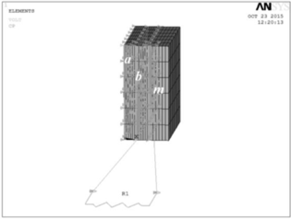 | Fig. 6. The ANSYS model with the same size as that used in the theoretical analyses. |
The electrical conductances calculated from the two electrodes of plate a with plate b shunted to different values of a resistor, a capacitor and an inductor in series with a resistor (0.03 Ω) are calculated. The 0.03-Ω resistor is used to simulate the inner resistance of the conductor. The curves which correspond to the same values of SRR, SCR, and SLR as those of theoretical analyses are depicted in Figs.
In order to further verify the theoretical analytical results and the finite element results, an experimental prototype resonator is fabricated as shown in Fig.
 | Fig. 7. Prototype system: (a) the sample; (b) the finite element model. |
In the experiments, the conductance curves of the system with plate b shunted to different resistors, capacitors and inductors are tested by an impedance analyzer and shown in Figs.
 | Fig. 8. Electrical conductances of the system measured from the two electrodes of wafer a by experiments with b shunted to: (a1) a resistor (experiment); (a2) a resistor (FEM); (b1) a capacitor (experiment); (b2) a resistor (FEM); (c1) an inductor (experiment); (c2) an inductor (FEM). |
To verify the experimental results of the actual sample which has a finite size, a finite element model with the same size of the sample and a bonding layer is also established to conduct the simulations, as shown in Fig.
With an impedance analyzer, the conductance curves of the experimental sample are tested from two electrodes of plate a, with b shunted to different elements. The relationships between the resonant frequency of the sample and different shunted element values of a resistor, a capacitor and an inductor are measured respectively. Correspondingly, the relationships between the variations of the real part c55r of the TSM elastic constant c55 and the shunt circuits are obtained indirectly according to linear relations in Fig.
The experimental results are shown as the curves marked with ‘*’ in Figs.
 | Fig. 9. Relationships between the elastic constant c55r and (a) SRR, (b) SCR, and (c) SLR, respectively. |
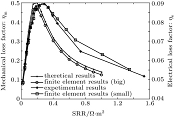
From Fig. 


As the resistance is the only way to dissipate energy and has an effect on the damping of the piezoelectric material, the relationship between the mechanical loss factor and SRR is worth investigating. In the experiment, the conductance curves of the experimental sample are tested for different values of a resistor with an impedance analyzer. The relationship between electrical loss factor ηe and SRR is first obtained, calculated with the relative bandwidth Δf/fr. The relationship between electrical loss factor ηe and SRR is first obtained, calculated with the relative bandwidth ηm. The relationship between electrical loss factor ηe and SRR is derived indirectly according to Fig.
 | Fig. 10. Relationships between mechanical loss factor ηm and SRR. |
In this paper, we propose a coupling electro–mechanical resonant system to indirectly measure the TSM elastic constant c55 and the mechanical loss factor ηm. Based on this model, the variation of the TSM elastic constant c55 of shear-mode piezoelectric ceramic with shunt circuit is investigated through the theoretical analysis with Mason equivalent circuit, and the variations of the mechanical loss factor and the resistance with shunt circuit is also studied, which are both verified by the FEM simulations. Since the changes of the resonant frequency and the bandwidth of the peak of the conductance are easily observed, the corresponding changes of the elastic constant c55 and the mechanical loss factor ηm can be obtained indirectly.
An experiment sample is fabricated with PZT5A to test the admittance of the system with an impedance analyzer. The theoretical and simulated results are verified experimentally. The variations of the TSM elastic constant c55 and the mechanic loss factor ηm with shunt element are obtained experimentally. The relative changes of the resonant frequency and bandwidth of resonant peak with the shunt circuits experimentally show that they are in good agreement with the theoretical analyses and FEM simulations correspondingly, indicating the validity of the proposed method of measuring the variations of the TSM elastic constant c55 and the mechanic loss factor ηm of shear-mode PZT5A shunted to different circuits. It should be pointed out that the proposed coupling resonator and the obtained relationships are validated with shear-mode PZT5A (but not limited only to PZT5A).
| 1 | |
| 2 | |
| 3 | |
| 4 | |
| 5 | |
| 6 | |
| 7 | |
| 8 | |
| 9 | |
| 10 | |
| 11 | |
| 12 | |
| 13 | |
| 14 | |
| 15 | |
| 16 | |
| 17 | |
| 18 | |
| 19 | |
| 20 | |
| 21 | |
| 22 | |
| 23 | |
| 24 | |
| 25 | |
| 26 | |
| 27 | |
| 28 | |
| 29 | |
| 30 |