† Corresponding author. E-mail:
Project supported by the National Key Research and Development Program of China (Grant No. 2016YFB0402204), the High-Tech Research and Development Program of China (Grant Nos. 2013AA031401, 2015AA016902, and 2015AA016904), and the National Natural Science Foundation of China (Grant Nos. 61674136, 61176053, 61274069, and 61435002).
Graphene is an alternative material for photodetectors owing to its unique properties. These include its uniform absorption of light from ultraviolet to infrared and its ultrahigh mobility for both electrons and holes. Unfortunately, due to the low absorption of light, the photoresponsivity of graphene-based photodetectors is usually low, only a few milliamps per watt. In this letter, we fabricate a waveguide-integrated graphene photodetector. A photoresponsivity exceeding 0.11 A·W−1 is obtained which enables most optoelectronic applications. The dominating mechanism of photoresponse is investigated and is attributed to the photo-induced bolometric effect. Theoretical calculation shows that the bolometric photoresponsivity is 4.6 A·W−1. The absorption coefficient of the device is estimated to be 0.27 dB·μm−1.
Graphene, one layer of carbon atoms arranged in a hexagonal lattice, has received tremendous research interest since its first realization.[1] Graphene-based devices, such as transistors,[2–4] gas sensors[5] and optical modulators[6–8] exhibit a number of merits. Particularly, owing to its extremely high mobility for both electrons and holes[9] and its uniform light absorption coefficient (∼2.3%) over a wide range of spectrum from ultraviolet to infrared,[10,11] different kinds of graphene-based photodetectors have been designed and fabricated.[12–25] The field-effect-transistor-structure graphene photodetectors are the most common ones.[12–14] However, since the photo-generated electrons and holes can be separated only in the vicinity of the metal leads (∼ 200 nm), its photoresponsivity is rather low, only a few milliamps per watt.[12] To improve the interaction between graphene and light, microcavity integrated graphene photodetectors are realized and a responsivity of 21 mA·W−1 is obtained.[23,24] However, this type of graphene photodetector requires a rather complicated fabrication process such as epitaxial growth of Bragg mirror and buffer layers.[24] An alternative way to acquire high photoresponsivity is a waveguide-integrated graphene photodetector, which enhances the absorption efficiency and lengthens the absorption length along the waveguide.[25] Recently, Li et al. experimentally reported a maximum of absorption coefficient of 0.2 dB·μm−1 by locating graphene directly on the top of a waveguide.[26] In this letter, we fabricate a waveguideintegrated graphene photodetector using a wet transfer method to transfer an individual graphene microsheet to the specific position of a waveguide. A photoresponsivity exceeding 0.11 A·W−1 is obtained which enables most optoelectronic applications. There are several different processes that convert photons into an electrical signal in graphene. These involve the photovoltaic effect, the photothermoelectric effect, and the bolometric effect. The dominating mechanism of photoresponse is investigated and is attributed to the photo-induced bolometric effect. Theoretical calculation shows that the bolometric photoresponsivity is 4.6 A·W−1. The absorption coefficient of the device is estimated to be 0.27 dB·μm−1, which is consistent with Li’s result.
The device fabrication starts with a wet transfer process. Briefly, a graphene sample is mechanically exfoliated on a Si/SiO2 substrate. Then a layer of poly (methyl methacrylate) (PMMA) is spin-coated on the Si/SiO2 substrate. Then the PMMA membrane is released in 1 mol·L−1 NaOH solution at 80 °C. The released PMMA membrane is then thoroughly cleaned in deionized water and dried in N2 flow. Then it is fixed to a home-made micrometer manipulator. Synchronously, a standard electron-beam lithography (EBL) is performed on the target substrate to pattern a transfer window for the graphene sample. Then the target substrate, with a drop of deionized water on its surface, is located on the wafer carrier of a microscope. Then the PMMA membrane and the target substrate are brought into contact. By adjusting the micrometer manipulator and the wafer carrier of the microscope, we can align the graphene sample to the target position. Once aligned, the whole set up is left in ambient condition for 12 hours. To further increase the interaction between the graphene sample and the substrate, the substrate is baked at 120 °C for 15 minutes. Then, it is cleaned in acetone, ethanol, and deionized water, leaving the graphene sample on the target position. The electrodes are fabricated by EBL followed by electron-beam evaporation (EBE) of 20 nm Ti and 70 nm Au. Finally, the device is thermally annealled in H2 and Ar mixture flow at 400 °C for 2 hours.
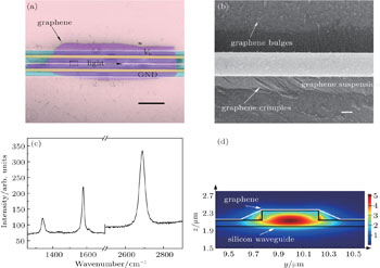
A false-color top-view scanning-electron-microscope (SEM) image of the device is shown in Fig.
The light source is a DFB laser operating at 1550 nm, amplified by EDFA and calibrated by an optical power meter (10 mW). Light is coupled in and out of the waveguide through two gratings which are designed particularly for a wavelength of 1550 nm. The coupling coefficient of each grating is measured to be 14%, corresponding to an incident power of 1.4 mW in the waveguide. Figure
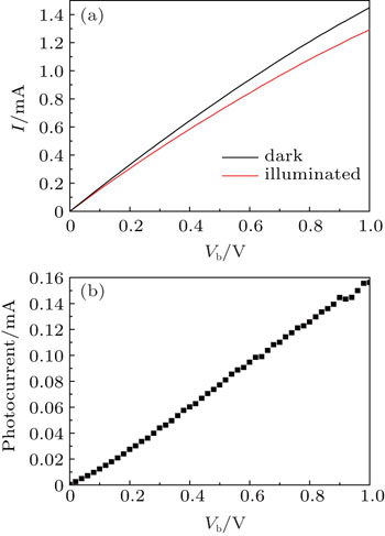
Current I as a function of bias voltage Vb with and without illumination is plotted in Fig.
We now move on to discuss the photoresponse mechanism of the device. Generally, there are three effects that contribute to the photocurrent. The first is the photovoltaic effect (PVE) where light-excited electrons and holes are driven in opposite directions and are collected by electrodes within their lifetime, producing the photocurrent.[12–16] However, this is obviously not the dominant photocurrent mechanism of the device, since if so there should be an increase rather than a reduction of current when illuminated. Therefore the photovoltaic effect is negligible in our device.
 | Fig. 2. (a) Current I as a function of bias voltage Vb with and without illumination. (b) The photocurrent versus Vb curve. Vb is limited within 1 V. |
The second is the photo-thermoelectric effect (PTE), where according to the Seebeck effect, both temperature gradient and chemical potential gradient generate a thermoelectric current.[17–20] In the case of our device, light absorption generates the temperature gradient perpendicular to the waveguide and electrical bias breaks the balance of the chemical potential gradient although graphene is homogenously doped. The photocurrent generated by PTE is determined by


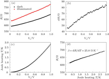
The only possible explanation of our observation is the photo-bolometric effect (PBE), where light absorption elevates the local temperature of graphene by strong electron-phonon interaction, which in turn enhances the electron-acoustic phonon scattering, leading to an increase of resistance, i.e., a reduction of current.[21,30] Since PBE is resistance related, we thus convert Fig.
In conclusion, we have fabricated a waveguide-integrated graphene photodetector using a wet transfer method to transfer an individual graphene microsheet to the specific position of a waveguide. A photoresponsivity exceeding 0.11 A·W−1 is obtained which enables most optoelectronic applications. The mechanism of the photoresponse is investigated and is attributed to the photo-induced bolometric effect. Theoretical calculation shows that the bolometric photoresponsivity is 4.6 A·W−1. The absorption coefficient of the device is estimated to be 0.27 dB·μm−1.
| 1 | |
| 2 | |
| 3 | |
| 4 | |
| 5 | |
| 6 | |
| 7 | |
| 8 | |
| 9 | |
| 10 | |
| 11 | |
| 12 | |
| 13 | |
| 14 | |
| 15 | |
| 16 | |
| 17 | |
| 18 | |
| 19 | |
| 20 | |
| 21 | |
| 22 | |
| 23 | |
| 24 | |
| 25 | |
| 26 | |
| 27 | |
| 28 | |
| 29 | |
| 30 | |
| 31 | |
| 32 |


