Bolometric effect in a waveguide-integrated graphene photodetector
Wang Yubing, Yin Weihong, Han Qin†,  , Yang Xiaohong, Ye Han, Lv Qianqian, Yin Dongdong
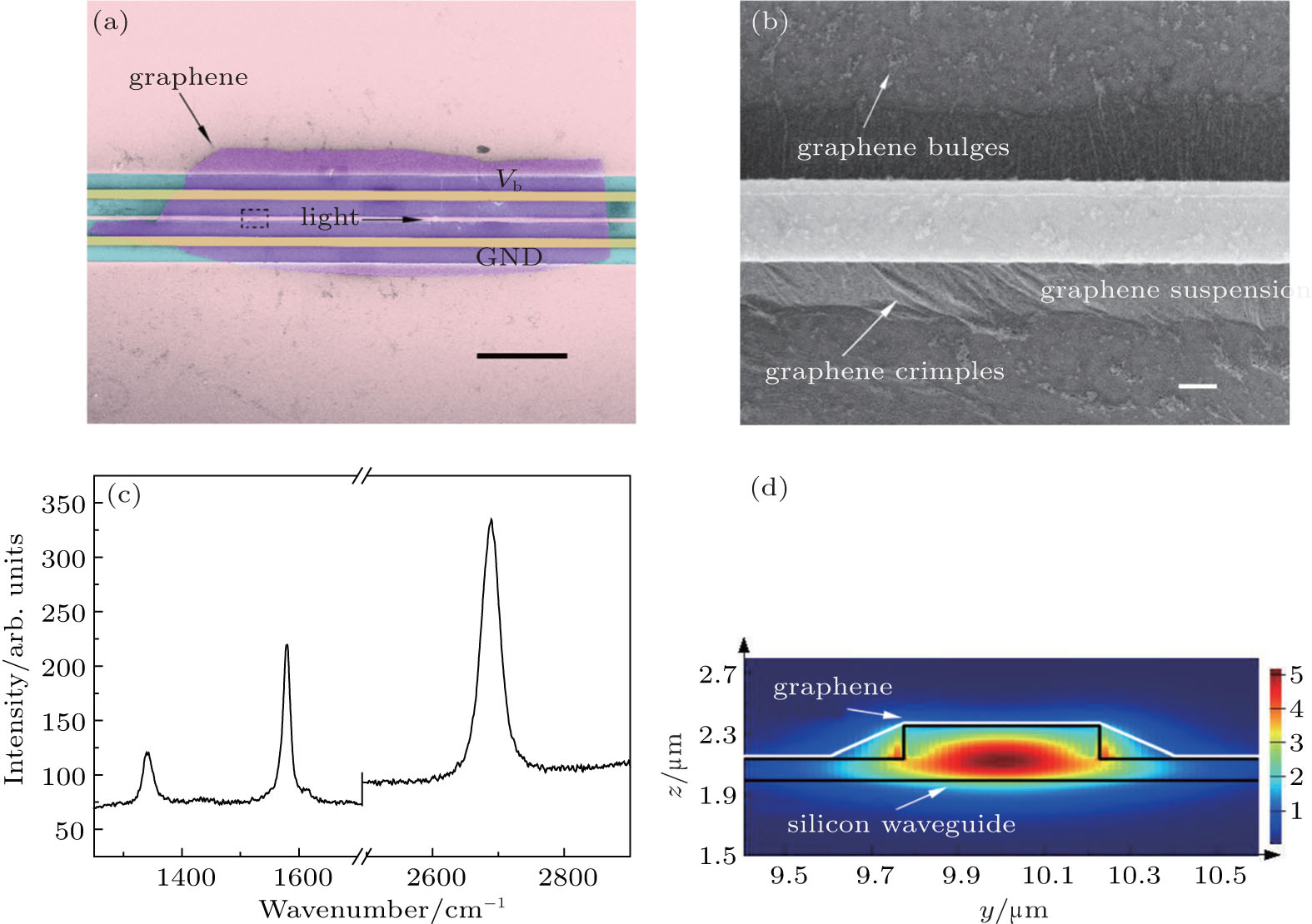
, Yang Xiaohong, Ye Han, Lv Qianqian, Yin Dongdong (a) A false-color topview SEM image of the device, displaying graphene (purple), metal leads (yellow), unetched silicon (pink), and etched region (green). Scale bar, 10 μm. (b) A zoom-in view of the region indicated by dash box in Fig.