Research of the use of silver nanowires as a current spreading layer on vertical-cavity surface-emitting lasers
Guo Xia1, †, , Shi Lei2, Li Chong1, ‡, , Dong Jian2, Liu Bai2, Hu Shuai2, He Yan2
School of Electronic Engineering, Beijing University of Posts and Telecommunications, Beijing 100876, China
Photonic Device Research Laboratory, Institute of Electronic Information and Control Engineering, Beijing University of Technology, Beijing 100124, China


† Corresponding author. E-mail: guo@bjut.edu.cn

‡ Corresponding author. E-mail: lichong@bjut.edu.cn

Project supported by the National Natural Science Foundation of China (Grant Nos. 61335004 and 61505003), the National High Technology Research and Development Program of China (Grant No. 2015AA017101), and the National Key Research and Development of China (Grant No. 2016YFB0400603).

Abstract
Abstract

Silver nanowire (AgNW) film was proposed to apply on the surface of the vertical-cavity surface-emitting lasers (VCSELs) with large aperture in order to obtain a uniform current distribution in the active region and a better optical beam quality. Optimization of the AgNW film was carried out with the sheet resistance of 28.4 Ω/sq and the optical transmission of 94.8% at 850 nm. The performance of VCSELs with and without AgNW film was studied. When the AgNW film was applied to the surface of VCSELs, due to its better current spreading effect, the maximum output optical power increased from 23.4 mW to 24.4 mW, the lasing wavelength redshift decreased from 0.085 nm/mA to 0.077 nm/mA, the differential resistance decreased from 23.95 Ω to 21.13 Ω, and the far field pattern at 50 mA decreased from 21.6° to 19.2°. At the same time, the near field test results showed that the light in the aperture was more uniform, and the far field exhibited a better single peak characteristic. Various results showed that VCSELs with AgNW on the surface showed better beam quality.

1. Introduction

By virtue of the structural characteristics, vertical-cavity surface-emitting lasers (VCSELs) have the advantages of high efficiency, low divergence angle, easy to fabricate into two-dimensional arrays, etc.[13] Recently, VCSELs with apertures larger than 100 μm have found new applications as a pumping source due to their high output optical power. However, it is difficult to obtain a better optical beam quality due to the non-uniform current distribution in the active region, which then causes a non-uniform gain and the filament phenomenon in the far field pattern of the lasers.[4] The crowding of carriers at the aperture’s edge will also cause Joule heating and then bent-down of the optical output power. Hence, improving the current distribution uniformity in the active region is important for obtaining higher output power and better optical beam quality from VCSELs with large aperture.

Increasing the doping concentration of the p-type distributed Bragg reflectors (DBR) could improve the carrier’s lateral spreading, while this would increase the light absorption loss. At present, different kinds of electrode structures have been used to improve the current spreading in the active region. For example, the radiation bridge electrode has been used instead of the traditional ring electrode.[5] Optimizing the size and the shape of the bottom electrode and the distance between the top and the bottom electrodes could also reduce the current density at the boundary of the active region.[6] ITO, which was widely used in the LED field, was applied in GaN VCSELs due to the relatively low doping concentration of the p-type GaN, which could effectively increase the carrier distribution uniformity.[7] However, indium is a precious resource. Many nanometer materials have been proposed to replace ITO.[810]

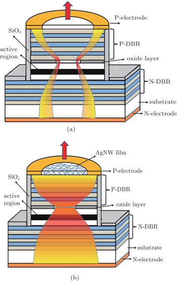
In this paper, a silver nanowire (AgNW) film with the sheet resistance of 28.4 Ω/sq and the optical transmission of 94.8% at 850 nm was proposed to apply on the VCSELs’ surface to improve the uniformity of the carriers in the active region, as shown in Fig. 1. The maximum output optical power was increased from 23.4 mW to 24.4 mW and the optical beam quality was improved significantly when the AgNW film was applied to the surface of VCSELs.

Fig. 1. Schematic cross sections of VCSELs with the illustration of the current flow in the devices: (a) VCSELs without AgNW film on the top surface, (b) VCSELs with AgNW film on the top surface. The current flow in the VCSELs with AgNW film on the top surface is more uniform.
2. Structure and fabrication of the device

The VCSELs’ structure was grown on an n-type GaAs substrate by the metal organic vapor phase deposition. The bottom n-type DBR contained 34.5 pairs Si-doped Al0.9Ga0.1As/Al0.12Ga0.88As for high optical reflectivity. The selection of 12% Al component was due to the lasing wavelength being designed to be 850 nm. Then, the undoped active region contained three GaAs/AlGaAs quantum wells centered at the anti-node of the optical standing wave within the one-wavelength cavity, with a photoluminescence peak at 835 nm. The top p-type DBR, above the active region, consisted of 20.5 pairs C-doped Al0.12Ga0.88As/Al0.9Ga0.1As. The graded interfaces, whose thickness was 20 nm, were used both on the top and the bottom DBR layers to reduce the differential resistance and maintain the low free carrier’s absorption loss. A single Al0.98Ga0.02As oxidization layer in the p-type mirror adjacent to the active region was employed to form the oxide aperture for voltaic and optical confinement. A highly doped 25 nm GaAs ohmic contact layer was grown on the top.

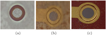
The Al0.98Ga0.02As layer was exposed by a wet etching process. The wet nitrogen oxidation process was then carried out in a furnace with a temperature of 400 °C, the N2 flow of 1 L/min, and a water temperature of 90 °C to obtain a low refractive index oxide layer for the carriers and light confinement. Figure 2(a) shows a microscope image of the Al0.98Ga0.02As layer after the oxidation process. The oxidation aperture, which could be measured under the microscope by the big difference in the refractive index between the oxide and the original Al0.98Ga0.02As layer, was about 42 μm and its oxidation rate was 0.65 μm/min. SiO2, whose thickness was 400 nm, was deposited on the surface by the plasma enhanced chemical vapor deposition method as a passivation layer. Ti/Au and AuGeNi/Au were deposited by sputtering as the anode and the cathode, respectively. After annealing, the AgNW solution with a concentration of 0.5 mg/ml was spin-coated onto the surface of the VCSEL’s device. After cleaving, the VCSELs’ chip was packaged onto the TO for the electrical and optical measurements at room temperature. Figures 2(b) and 2(c) demonstrate the microscope images of the device surface with and without AgNW film. The surface was smooth and clean before applying the AgNW film.

Fig. 2. (a) Microscope image of the Al0.98Ga0.02As layer after oxidation process. The color difference was caused by the large refractive index difference between the oxide and the original Al0.98Ga0.02As layer. (b), (c) The surfaces of the devices with and without AgNW film, respectively. The surface was smooth and clean before applying the AgNW film.

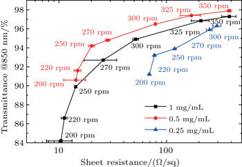
The Ag nanowires were prepared following the reported procedure.[11] In brief, 0.5 g glucose and 0.1 g polyvinyl pyrrolidone (PVP) were dissolved in 35 ml deionized water to form a solution. Then, 0.5 ml freshly prepared 0.1 M aqueous AgNO3 solution was added under vigorous stirring. The mixture was transferred into a 40 ml Teflon-sealed autoclave and heated at 140 °C for 10 h. After the reaction, the autoclave was allowed to cool in air and the product was purified by 3–5 centrifugation/rinsing/redispersion circles. Then, the AgNW re-dispersed in isopropyl alcohol due to better dispersibility for different concentrations. Figure 3 shows the relationships between the optical transmittance at 850 nm and the sheet resistance at the spin-coating speed of 200–350 rpm with the AgNW concentrations of 0.25 mg/ml, 0.5 mg/ml, and 1 mg/ml, respectively. For all the concentrations of AgNW, the transmission increased with the spin-coating speed due to little AgNW leaving on the surface. The sheet resistance increased with the transmission, which is a typical phenomenon known as the percolation effect. For the same spin-coating speed, the sheet resistance for the AgNW concentration of 1 mg/ml was the smallest. More metal nanowires helped to decrease the sheet resistance. However, more metal nanowires could block the light. Among all of these samples, the one with the AgNW concentration of 0.5 mg/ml had the highest transmission for the same sheet resistance, which was our optimized result. In our experiment, the sample with the transmission of 94.8% and the sheet resistance of 28.4 Ω/sq was selected, which was obtained at the spin-coating speed of 270 rpm/min and the concentration of 0.5 mg/ml.

Fig. 3. The relationships between the optical transmittance at 850 nm and the sheet resistance at the spin-coating speed of 200–350 rpm with the AgNW concentrations of 0.25 mg/ml, 0.5 mg/ml, and 1 mg/ml, respectively.
3. Test results analysis

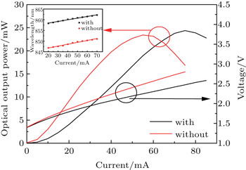
Figure 4 compares the LIV measurement results of the VCSELs with and without AgNW film. Under continuous current injection, the output optical power increased with the injection current and then bent down due to the Joule heating.[12] The maximum output optical power was 24.4 mW and 23.4 mW for the VSCELs with and without AgNW film, respectively. About 4.4% increase of output optical power was caused by the relief of the carrier congregation near the aperture. Due to the constant accumulation of heat in the active region and carriers crowed near the aperture, the optical power bending occurred earlier. Correspondingly, the threshold current was 6.23 mA and 3.15 mA, respectively, for the VCSELs with and without AgNW film. The increase of the threshold current was due to the optical loss and the decrease of the level of injection. Thus, a larger drive current was needed to achieve the lasing condition of population inversion. Consequently, it led to the increase of the threshold of the device. The optical output power was a little bit lower for the VCSELs with AgNW film under the same injection, which was possibly caused by the absorption loss of the AgNW film. Further evidence of the better current distribution came from the electrical performance. The voltage drop decreased from 2.41 V to 2.19 V at 50 mA and the differential resistance decreased from 23.95 Ω to 21.13 Ω due to the reduction of the lateral resistance, which happened because the carriers were more easily laterally transferred to the lateral position when the AgNW film was applied to the surface of the VCSELs. The dependence of the lasing wavelength of the VCSELs with and without AgNW film on the injection current is shown in the inset of Fig. 4. At 20 mA, the peak wavelengths were 858.3 nm and 846.8 nm, respectively. The lasing wavelength redshifted with the current injection due to the heating. The redshift rates were 0.077 nm/mA and 0.085 nm/mA for the VCSELs with and without AgNW film, respectively. The redshift rate reduced for the VCSELs with AgNW film because of the better current spreading effect and the better heat dissipation of the AgNW film. The thermal conductivity of silver is 429 W/(m·K) and the thermal conductivity of air is 0.03 W/(m·K), in other words there is a huge gap between the two. When the silver nanowires were laid on the VCSELs surface, the heat generated inside the device can be better distributed out, thereby reducing the red-shift rate.

Fig. 4. Comparison of LIV and the spectral measurement results at different injection currents for VCSELs with and without AgNW film. The inset shows the dependence of the lasing wavelength on the injection current for the VCSELs with and without AgNW film on the top surface. The maximum output optical power increased from 23.4 mW to 24.4 mW, the wavelength redshift decreased from 0.085 nm/mA to 0.077 nm/mA, and the differential resistance decreased from 23.95 Ω to 21.13 Ω.

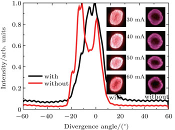
The near field patterns of the VCSELs with and without AgNW film under the injection current of 30–60 mA are demonstrated in the inset of Fig. 5, which were measured under the microscope. For the VCSELs without AgNW film, the light almost emitted from the edge of the oxide aperture, while the center of the aperture was almost dark. For the VCSELs with AgNW film, the light in the aperture was more uniform due to the better carrier distribution in the active region. Correspondingly, the far field patterns were 19.2° and 21.6° for the VCSELs with and without AgNW film at 50 mA, respectively, as shown in Fig. 5. There was an obvious split in the center of the far field pattern for the VCSELs without AgNW, which decreased the optical beam quality. The far field test results showed that the spot had a better single peak characteristic.

Fig. 5. The far field patterns of the devices with and without AgNW film under the injection current of 50 mA. The inset is the near field images measured by microscope under the injection current of 30–70 mA.
4. Conclusion

VCSELs with and without AgNW film on the top surface were fabricated with a sheet resistance of 28.4 Ω/sq and an optical transmission of 94.8% at 850 nm. Due to the relief of the carrier crowding effect, the maximum output power increased from 23.4 mW to 24.4 mW and the wavelength redshift decreased from 0.085 nm/mA to 0.077 nm/mA. Uniform near field images were obtained under current injection from 30 mA to 70 mA. Correspondingly, the far field pattern at 50 mA decreased from 21.6° to 19.2°. The various results showed that VCSELs with AgNW on the surface showed better beam quality.

Reference
1Yen J LChi K LJiang J WYang Y JShi J W 2014 IEEE Journal Of Quantum Electronics 50 787
2Wang W JLi CZhou H YWu HLuan X XShi LGuo X 2015 Chin. Phys. 24 024209
3Lu H HLin Y PWu P YChen C YChen M CJhang T W 2014 Opt. Express 22 3468
4Miller MGrabherr MKing RJager RMichalzik REbeling K J 2001 IEEE J. Sel. Top. Quantum Electron 7 210
5Hao Y QFeng YWang FYan C LZhao Y JWang X HWang Y XJiang H LGao XBao B X2011Acta Phys. Sin.60064201(in Chinese)
6Zhang XNing Y QZeng Y GZhang J LFu X HQin LLiu YTong C ZWang L J 2012 IEEE Journal Of Quantum Electronics 48 42
7Xu P2013Design and Research of Transparent Conductive Window of Vertical Cavity Surface Emitting Semiconductor Laser (MS Thesis)Changchun: Changchun University of Science and Technology(in Chinese)
8Krantz JRichter MSpallek SSpiecker EBrabec C J 2011 Adv. Funct. Mater. 21 4784
9Jeong JKim H 2014 Appl. Phys. Lett. 104 71906
10Khanarian GJoo JLiu XEastman PWerner DO’Connell KTrefonas P 2013 J. Appl. Phys. 114 24302
11Sun X MLi Y D 2005 Adv. Mater. 17 2626
12Larson M CKondow MKitatani TNakahara KTamura KInoue HUomi K 1998 IEEE Photonics Technology Letters 10 188