Apodized grating coupler using fully-etched nanostructures
Wu Hua1, 2, Li Chong1, Li Zhi-Yong3, Guo Xia1, 4, †,
Photonic Device Research Laboratory, College of Electronic Information and Control Engineering, Beijing University of Technology, Beijing 100124, China
College of Physics and Electronic Information, GanNan Normal University, Ganzhou 341000, China
State Key Laboratory for Integrated Optoelectronics, Institute of Semiconductors, Chinese Academy of Sciences, Beijing 100083, China
School of Science, Minzu University of China, Beijing 100081, China


† Corresponding author. E-mail: guo@bjut.edu.cn

Project supported by the National Natural Science Foundation of China (Grant Nos. 61222501, 61335004, and 61505003), the Specialized Research Fund for the Doctoral Program of Higher Education of China (Grant No. 20111103110019), the Postdoctoral Science Foundation of Beijing Funded Project, China (Grant No. Q6002012201502), and the Science and Technology Research Project of Jiangxi Provincial Education Department, China (Grant No. GJJ150998).

Abstract
Abstract

A two-dimensional apodized grating coupler for interfacing between single-mode fiber and photonic circuit is demonstrated in order to bridge the mode gap between the grating coupler and optical fiber. The grating grooves of the grating couplers are realized by columns of fully etched nanostructures, which are utilized to digitally tailor the effective refractive index of each groove in order to obtain the Gaussian-like output diffractive mode and then enhance the coupling efficiency. Compared with that of the uniform grating coupler, the coupling efficiency of the apodized grating coupler is increased by 4.3% and 5.7%, respectively, for the nanoholes and nanorectangles as refractive index tunes layer.

1. Introduction

Grating couplers, as one of the key elements enabling the light to be directly coupled between the planar waveguide circuits and the optical fibers, are widely used in the field of silicon photonic integrated circuits.[13] The coupling efficiency is limited by the scattering efficiency, the directionality and the mode matching degree between the exponential decline field of the upward diffracted field and the fundamental mode of the single-mode fiber (SMF).[4,5] The 100% scattering efficiency could be reached by designing a long enough grating that fulfills the Bragg condition at the target wavelength. The directionality can be avoided by using a metal mirror, or by optimizing the buried oxide (BOX) thickness through the interference effect inside the substrate layer.[6,7] By now, the main difficulty in further improving the coupling efficiency is the mode mismatch between the exponentially declined diffraction field and the Gaussian field of the SMF.[8] There is about 20% coupling efficiency loss caused by the mode mismatch. It is a challenge to bridging such a mode mismatch to further improve the coupling efficiency between the grating coupler and optical fiber. Many approaches have been proposed to increase the mode matching degree, such as the nonuniform etching depth of the grooves, nonuniform duty cycles by tuning the scattering efficiency of each groove.[810] However, the process is relatively complicated.

Recently, nanostructures have exhibited the feasibility of the effective refractive index tailoring according to the equivalent medium theory, which relaxes the refractive index limitation by the current bulk material.[11] Engineering the effective refractive index distribution of the gratings could modify the grating strength and then the profile of the diffraction light. Detailed design method for digitally apodized grating couplers with Gaussian diffractive mode has been published without considering any practical limitations.[12] With the back mirror, the calculated coupling efficiency of 93.1% at 1550 nm with 3-dB bandwidth of 82 nm can be achieved. The matching degree has reached 97.3% between the field profile of upward-diffracted light and optical fiber mode. However, the BOX thickness is 2.2 μm, which is unavailable commercially. Based on the equivalent medium theory, the two-section apodized subwavelength gratings were fabricated on a silicon-on-insulator (SOI) substrate. The calculated and measured peak coupling efficiency were 60.3% and 50.4% at about 1550 nm for TE mode, respectively.[13,14] Photonic crystal (PhC) structure was also employed to engineer the refractive index of each groove to improve the coupling efficiency.[15] The selection of the effective refractive index is determined by the hole size. The calculated and measured coupling efficiency of 66% and 67% for the TE mode were realized.[16] By bonding an aluminum mirror to employ the back reflection light, the coupling efficiency increased to about 87.5%.[17]

However, in practice, the width of the Gaussian mode is about 20 μm when the field intensity decreases to almost 0 according to the fitting of the Gaussian mode in the standard SMF with a full width (1/e) of 10.4 μm, which determines the total length of the grating. On the other side, suppression of the grating strength will increase the transmission loss for the commercial SOI substrate. Because the difference between the exponential decaying field and the Gaussian mode is large at the beginning of the grating, it is important to suppress the grating strength at the beginning. Figure 1 shows the simulation results of the dependences of the grating strength and transmittance on the effective refractive index of the grating grooves for a uniform grating coupler by using the finite difference time domain (FDTD) method. The transmittance through the uniform grating increases with neq while grating strength decreases with it as the neq is larger than around 2.5, which indicates that adequate suppression of the grating strength at the beginning of the gratings can increase the transmission loss and then reduce the total coupling efficiency. Transmission loss, not like downward-diffraction which can be employed by an additional mirror, cannot be recollected or reused. Hence, there is a balance between the mode overlap and total coupling efficiency.
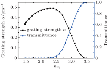
Fig. 1. Calculated dependences of the grating strength and transmittance on the effective refractive index of grating grooves.

The apodized grating couplers using fully etched both nanorectangles and nanoholes were fabricated by considering the transmittance loss. The coupling efficiencies are increased by 5.7% and 4.3%, respectively, compared with those of the uniform grating couplers at 1550 nm. Compared with a traditional shallowly etched grating coupler, the proposed apodized fully etched grating coupler with grating grooves realized by columns of fully etched nanostructures has two advantages. One is that with the feasibility of digital tailoring, the effective refractive index of each groove can obtain the Gaussian-like output diffractive mode. The other is that the fully etched grating coupler can simplify the fabrication process since it can be fabricated by using the same process as that for fabricating the strip waveguide.

2. Optimization of apodized grating couplers

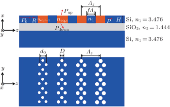
Figure 2 shows the cross-section (a) and top view (b) of the proposed apodized grating coupler. Our designed grating couplers are implemented in a standard 260-nm-thick SOI wafer with a 1-μm-thick BOX layer. The grating is optimized for transverse electric (TE) polarization and a central wavelength of 1550 nm. For the 1550-nm wavelength, the refractive index n1 = 3.476 for Si, n2 = 1.444 for SiO2. Each groove is composed of nanorectangles or nanoholes along the y direction with the effective refractive index of neq,i for the i-th period. Then the alternate two-dimensional (2D) nanostructures with bulk Si can be regarded as a conventional one-dimensional (1D) grating structure with alternative effective refractive index of the neq,i and n1, and longitudinal period Λz, duty cycle f, which is illustrated in Fig. 2(a).

Fig. 2. Schematic diagram of an apodized grating coupler with nanostructures serving as grating grooves: (a) side view; (b) top view.
Fig. 3. Value distributions of duty cycle of the i-th groove fy,i, equivalent refractive index neq,i of the grating grooves, and longitudinal grating period Λz,i for apodized grating couplers using nanorectangles as refractive index tuning layer, versus longitudinal grating period number.

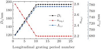
In order to obtain high coupling efficiency, the selection of the effective refractive index of each groove is determined by a large number of trials. Two-section grating couplers are determined with the first section as the effective refractive index linearly varies from 2.8 to 2.2 for the first 10 periods. The second section uses a uniform effective refractive index of 2.2 along 15 periods. The maximum effective refractive index is limited to 2.8 for the lower transmittance loss according to Fig. 1. The optimized distributions of the i-th groove fy,i, equivalent refractive index neq,i of the grating grooves, and longitudinal grating period Λz,i for apodized grating couplers using nanorectangles as refractive index tuning layer, versus the i-th longitudinal grating period number of duty cycle of the i-th groove fy,i are shown in Fig. 3. The value distributions of the i-th groove Di, equivalent refractive index neq,i of the grating grooves, and longitudinal grating period Λz,i for apodized grating couplers using nanoholes as refractive index tuning layer, versus longitudinal grating period number are shown in Fig. 4. neq,i and Λz,i distributions are the same for these two gratings. Trends of fy,i and Di are the opposite because neq,i is proportional to fy,i, but inversely proportional to Di. In order to compare the tuning effect of the effective refractive index on coupling efficiency, both the apodized and the uniform grating couplers are simulated and fabricated.

Fig. 4. Value distributions of the i-th groove Di, equivalent refractive index neq,i of the grating grooves, and longitudinal grating period Λz,i for apodized grating couplers using nanoholes as refractive index tuning layer, versus longitudinal grating period number.

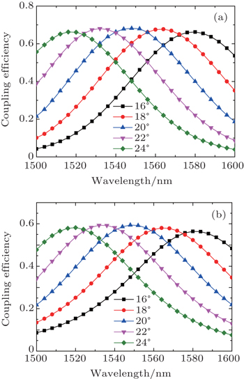
Figure 5 shows variations of coupling efficiencies with wavelength at incident angles of from 16 to 24, solved by the FDTD software for the apodized grating couplers (Fig. 5(a)) and uniform grating couplers (Fig. 5(b)). The neq of the uniform grating coupler is 2.4 because its coupling efficiency is maximum at 1550 nm according to the FDTD simulation result of the coupling efficiency dependent on the refractive index. The wavelengths at the peak coupling efficiency are almost the same: blue shifts with the incident angle both for the apodized and uniform grating couplers, which can be seen from the phase-matching conditions. The peak coupling efficiencies are 68.2% and 59.4%, with the 3-dB bandwidths of 74 nm and 80 nm for the apodized and uniform grating couplers, respectively. However, when the incident angle is 20°, the wavelength of 1550 nm reaches the peak coupling efficiency.

Fig. 5. Variations of coupling efficiency of apodized grating coupler (a) and uniform grating coupler with wavelength at neq = 2.4 of grating grooves (b), for different coupling angles.
3. Grating coupler fabrication and experimental results

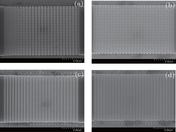
Figure 6 shows the scanning electron microscopy (SEM) images of the fabricated apodized and uniform grating couplers with nanorectangles and nanoholes as refractive index tuning layer, which are fabricated on an SOI wafer with a top silicon thickness of 260 nm and BOX layer thickness of 1 μm. After e-beam lithography and the inductively coupled plasma (ICP) etching patterned the nanostructures according to the design parameters, the silicon waveguides are formed by the traditional ultraviolet lithography and ICP etching with SF6/C4F8 gases. All these grating couplers are connected with a 1-mm-long and 12 μm-wide waveguide serving as input and output optical power measurement interfaces. The coupling efficiency is then determined as square root of the ratio between the output and input optical power since the waveguide losses can be ignored.[6] It should be pointed out that the purpose of a fully etched grating coupler is to simplify the fabrication processes since it can be fabricated by using the same process as that for fabricating the strip waveguide. In our paper, the fully etched grating coupler and the strip waveguide are fabricated separately due to the cost. The application of two-step etching process does not affect the experimental results.

Fig. 6. SEM images of the fabricated apodized (a) and uniform (b) grating coupler with nanorectangles, apodized (c) and uniform (d) grating coupler with nanoholes.

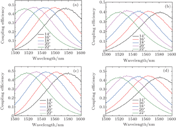
Figure 7 shows the measured variations of coupling efficiency with wavelength for the apodized and uniform grating couplers with nanorectangles and nanoholes at the coupling angles ranging from 14° to 22°. Also as shown in Fig. 7, the peak coupling efficiencies keep almost unchanged with the coupling angle, which indicates that the coupling wavelength shifting can be compensated for by fine adjusting the coupling angle. 2° coupling angle shifting will result in a 16-nm wavelength shift, which is in agreement with the simulation results as presented in Fig. 5. At 1532 nm and 1531 nm, the peak coupling efficiencies are 47.5% and 41.8% with 3-dB bandwidth of 67 nm and 69 nm, respectively, for the apodized and uniform grating couplers with nanorectangles as the refractive index tuning layers as shown in Figs. 7(a) and 7(b). While with nanoholes as the refractive index tuning layer, at 1534 nm and 1531 nm, the peak coupling efficiencies are 49.5% and 45.2% with 3-dB bandwidths of 69 nm and 73 nm, respectively as shown in Figs. 7(c) and 7(d). Compared with those of the uniform grating couplers, the coupling efficiencies of the apodized grating couplers are increased by 4.3% and 5.7%, respectively, for the nanoholes and nanorectangles as refractive index tuning layer. The improved coupling efficiency benefits from the better mode matching between the diffraction field distribution of apodized grating couplers and the mode field distribution of fiber. However, the measured peak coupling efficiency decreases a lot compared with the simulation results. We attribute it to the ICP processing because a smooth interface helps reduce the interface loss. The difference in the coupling efficiency between the apodized grating coupler with nanoholes and that with nanorectangles as refractive index tuning layer perhaps is caused by the deformation of the nanorectangles during the e-beam writing and etching, which is shown in Fig. 6. The coupling efficiency is a little bit lower than the simulation result, which is limited by the level of fabrication process of our laboratory.

Fig. 7. Measured coupling efficiencies versus wavelength of apodized (a) and uniform (b) grating coupler with nanorectangles, apodized (c) and uniform (d) grating coupler with nanoholes, for different coupling angles.
4. Conclusions

In this work, the apodized grating couplers by using nanorectangles and nanoholes to digitally tailor the effective refractive index of each groove are demonstrated, which is to bridge the mode gap between the grating coupler and optical fiber. The maximum coupling efficiency of 49.5% with 3-dB bandwidth of 69 nm is reached. Compared with that of the uniform grating couplers, the coupling efficiencies of the apodized grating couplers are increased by 4.3% and 5.7%, respectively, for the nanoholes and nanorectangles as refractive index tuning layer. The improved coupling efficiency benefits from the better mode matching between the grating couplers and SMF.

Reference
1Baehr-Jones TPinguet TGuo-Qiang P LDanziger SPrather DHochberg M 2012 Nat. Photon. 6 206
2Xu D XSchmid J HReed G TMashanovich G ZThomson D JNedeljkovic MChen XThourhout D VKeyvaninia SSelvaraja S K2014IEEE J. Sel. Top. Quantum Electron.208100217
3Dobbelaere P D201318th Asia and South Pacific Design Automation Conference644
4Roelkens GVermeulen DSelvaraja SHalir RBogaerts WThourhout D V 2011 IEEE J. Sel. Top. Quantum Electron. 17 571
5Yang BLi Z YYu Y DYu J Z 2014 Chin. Phys. 23 114206
6Zaoui W SRosa M FVogel WBerroth MButschke JLetzkus F 2012 Opt. Express 20 B238
7Van Laere FRoelkens GAyre MSchrauwen JTaillaert DThourhout D VKrauss T FBaets R 2007 J. Lightwave Technol. 25 151
8Zaoui W SKunze AVogel WBerroth MButschke JLetzkus FBurghartz J 2014 Opt. Express 22 1277
9Halir RCheben PJanz SXu D XMolina-Fernández ÍWangüemert-Pérez J G 2009 Opt. Lett. 34 1408
10Tang YWang ZWosinski LWestergren UHe S 2010 Opt. Lett. 35 1290
11Lalanne PLemercier-Lalanne D 1996 J. Mod. Opt. 43 2063
12Wu HLi CLiu QLiu BDong JShi LGuo X 2015 Chin. Opt. Lett. 13 050501
13Benedikovic DCheben PSchmid J HXu DJean LWang SHalir ROrtega-Monux AJanz SDado D 2014 Laser Photon. Rev. 8 L93
14Benedikovic DCheben PSchmid J HXu DLapointe JWang SJanz SHalir ROrtega-Monux ADado M 2015 Proc. SPIE 9516 95160I
15Liu LPu MYvind KHvam J M 2010 Appl. Phys. Lett. 96 051126
16Ding Y HOu H YPeucheret C 2013 Opt. Lett. 38 2732
17Ding Y HPeucheret COu H YYvind K 2014 Opt. Lett. 39 5348