


Impurity effects on electrical conductivity of doped bilayer graphene in the presence of a bias voltage
[Lotfi E1, †,  , Rezania H2, Arghavaninia B3, Yarmohammadi M4]
, Rezania H2, Arghavaninia B3, Yarmohammadi M4]
|
|


† Corresponding author. E-mail:
We address the electrical conductivity of bilayer graphene as a function of temperature, impurity concentration, and scattering strength in the presence of a finite bias voltage at finite doping, beginning with a description of the tight-binding model using the linear response theory and Green’s function approach. Our results show a linear behavior at high doping for the case of high bias voltage. The effects of electron doping on the electrical conductivity have been studied via changing the electronic chemical potential. We also discuss and analyze how the bias voltage affects the temperature behavior of the electrical conductivity. Finally, we study the behavior of the electrical conductivity as a function of the impurity concentration and scattering strength for different bias voltages and chemical potentials respectively. The electrical conductivity is found to be monotonically decreasing with impurity scattering strength due to the increased scattering among electrons at higher impurity scattering strength.
Electrons in bilayer graphene exhibit quite unusual properties: they can be viewed as massive chiral fermions with a parabolic dispersion at intermediate energies and have Berry phase 2π;[1,2] in contrast, the charge carriers in monolayer graphene are Berry-phase-π quasiparticles with a linear dispersion.[3,4] In bilayer graphene (BLG), two coupled hexagonal lattices of carbon atoms are arranged according to simple and Bernal stacking.[1,5–9] Because BLG has a large degeneracy at the charge neutral point,[1,5–9] there have been intense discussions on the possible many-body effects in the system.[10–15] Moreover, since electrons in single layer graphene (SLG) behave as relativistic massless fermions,[9] BLG provides a unique play ground to control the interactions between relativistic particles and relative mechanical motions of two layers. The electronic structure of bilayer graphene was studied theoretically and the spectrum was found to be essentially different from that of monolayer graphene.[1] In addition to interesting underlying physics, bilayer graphene holds potential for electronic applications, not only because of the possibility to control both carrier density and energy band gap through doping or gating.[1,8,16–20] Not surprisingly, many of the properties of bilayer graphene are similar to those of monolayer graphene.[9,21] These include an excellent electrical conductivity with room temperature mobility up to 40000 cm2· V−1· s−1 in air,[22] the possibility to tune the electrical properties by changing the carrier density through gating or doping,[17,23,24] a high thermal conductivity with room temperature thermal conductivity about 2800 W· m−1· K−1,[25,26] mechanical stiffness, strength, flexibility (Young’s modulus is estimated to be about 0.8 TPa[27,28]), transparency with transmittance of white light of about 95%,[29] impermeability to gases,[30] and the ability to be chemically functionalised.[31] Thus, as monolayer graphene, bilayer graphene has potentials for future applications in many areas,[21] including transparent, flexible electrodes for touch screen displays,[32] high-frequency transistors,[33] thermoelectric devices,[34] plasmonic devices,[35] photodetectors,[36] batteries,[37,38] and composite materials.[39,40] It should be stressed, however, that bilayer graphene has features that make it distinct from monolayer graphene. Like monolayer graphene, intrinsic bilayer graphene has no band gap between its conduction and valence bands, but the low-energy dispersion is quadratic (rather than linear in monolayer graphene) with massive chiral quasiparticles[1,2] rather than massless ones. As there are only two layers, bilayer graphene represents the thinnest limit of an intercalated material.[37,38] It is possible to address each layer separately leading to entirely new functionalities in bilayer graphene, including the possibility to control an energy band gap of up to about 300 meV through doping or gating.[1,8,16–20]
In contrast to the case of SLG, low energy excitations of the bilayer graphene have a parabolic spectrum, although the chiral form of the effective two-band Hamiltonian persists because the sublattice pseudospin is still a relevant degree of freedom. The low energy approximation in bilayer graphene is valid only for small doping n < 1012 cm−2, while experimentally doping can obtain 10 times larger densities. For such a large doping, the 4-band model[1] should be used instead of the low energy effective two-band model. Bilayer graphene is of intense interest as it too shows an unusual quantum Hall effect[1,41] and indeed its low energy tight-binding Hamiltonian maps to an equation for chiral fermions with an effective mass based on an interlayer hopping parameter γ. Graphene is an extremely flexible material from the electronic point of view and the electronic gap can be controlled. This can be accomplished in a graphene bilayer with an electric field applied perpendicular to the plane. It was shown theoretically[1,18] and demonstrated experimentally[20,42] that the graphene bilayer is the only material with semiconducting properties that can be controlled by the electric field effect.[8] The gap between the conduction and valence bands is proportional to the voltage drop between the two graphene planes and can be as large as 0.1–0.3 eV, allowing for novel THz devices[20] and carbon based quantum dots[43] and transistors.[44] Bilayer graphene is sensitive to the unavoidable disorder generated by the environment of the SiO2 substrate: adatoms, ionized impurities, etc. In this context, it is worth mentioning the transport theories based on the Boltzman equation,[45] a study of weak localization in bilayer graphene,[46] and also the corresponding further experimental characterization.[47] The static transport in few-layer graphene has been studied for both without and in the presence of a magnetic field. Thermopower of clean and impure biased bilayer graphene has been calculated for Bernal AB-stacking within the Born approximation.[48]
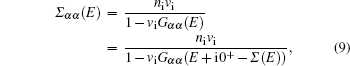
In our previous work, we studied the transport properties of clean bilayer graphene in the presence of a biased voltage.[49,50] In this paper, we study the effects of site dilution or unitary scattering and bias voltage on the electrical conductivity of both AA and AB stacked graphene bilayers within the well-known self-consistent Born approximation (SCBA).[48] This approximation allows for analytical results of electronic self-energies, allowing us to compute physical quantities such as spectral functions measured by angle resolved photoemission[51,52] and density of states measured by scanning tunneling microscopy,[53,54] besides the standard transport properties such as the direct-current (DC) and alternating-current (AC) conductivities. To ensure the applicability of SCBA, we restrict our calculations to relatively clean systems with low impurity concentrations. The electrical conductivity of two different stacked bilayer graphene as a function of the impurity concentration is calculated for different bias voltages and scattering potential strengths. We also study the effects of the impurity concentration and scattering potential strength on the temperature dependence of the electrical conductivity in bilayer grapehene.
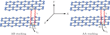
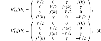
We start from a tight-binding model incorporating the nearest neighboring intralayer and interlayer hopping terms. An on-site potential energy difference between the two layers is included to model the effect of an external voltage. For the case of AA-stacking,[44] an A (B) atom in the upper layer is stacked directly above the A (B) atom in the lower layer. The nearest neighbor tight-binding model Hamiltonians for AA-stacked bilayer grapehene 

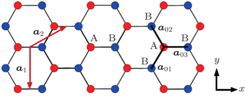
The first two terms are the nearest neighbor intralayer hopping terms for electrons to move within a given plane with hopping energy t∥ ≈ 3 eV. The two planes are indexed by 1 and 2. According to the crystal structure of the honeycomb lattice, each layer has two inequivalent atoms labeled as A and B. The lattice structures of bilayer grapehene and single-layer grapehene are shown in Figs.


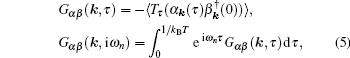
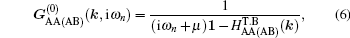


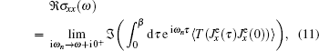
In the following, the expression for the electrical conductivity of bilayer graphene is presented using Green’s function method.[56] The Kubo formula gives us the in-plane dynamical electrical conductivity (σxx) in terms of the correlation function between electrical currents[56]


 | Fig. 1. The structure of bilayer. Both intra and inter layer hopping integrals are introduced in this figure. |
After substituting Eq. (


In the next section, the results of electrical conductivity for AA and AB stacked bilayer graphene are presented.
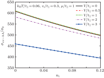
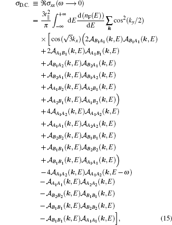
We obtain the electrical conductivity of the impurity doped AA stacked bilayer graphene along the x direction, as shown in Fig.
 | Fig. 2. The honeycomb structure. The light dashed lines denote the Bravais lattice unit cell. Each cell includes two nonequivalent sites, which are indicated by A and B. |
In Fig.
 | Fig. 3. Normalized electrical conductivity σxx/σ0 of biased doped AA stacked bilayer graphene as a function of impurity concentration ni for different bias voltages V/t∥ for vi/t∥ = 0.3. The normalized temperature is assumed to be kBT/t∥ = 0.06. |
The effect of the impurity concentration on the temperature behavior of the electrical conductivity of the AA stacked bilayer graphene in the presence of bias voltage V/t = 0.6 for vi/t∥ = 0.3 is shown in Fig.
 | Fig. 4. Normalized electrical conductivity σxx/σ0 of biased doped AA stacked bilayer graphene as a function of temperature kBT/t∥ for different impurity concentrations ni for vi/t∥ = 0.3. The normalized chemical potential is assumed to be μ/t∥ = 1.0. |
In Fig.
 | Fig. 5. Normalized electrical conductivity σxx/σ0 of biased doped AA stacked bilayer graphene as a function of temperature kBT/t∥ for different scattering strengths vi/t∥ for ni = 0.05. The normalized bias voltage is assumed to be V/t∥ = 1.25. |
 | Fig. 6. Normalized electrical conductivity σxx/σ0 of biased doped AB stacked bilayer graphene as a function of impurity concentration ni for different bias voltages V/t∥ for vi/t∥ = 0.3. The normalized temperature is assumed to be kBT/t∥ = 0.06. |
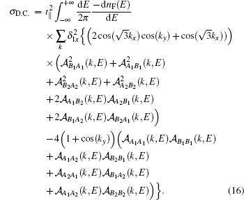
The electrical conductivity of the AB stacked bilayer graphene (σAB−stacked/σ0) versus the impurity concentration for different bias voltages at kBT/t∥ = 0.06 is shown in Fig.
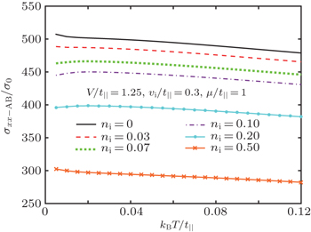
We have also studied the effect of impurity concentration ni on the temperature behavior of σAB−stacked/σ0. In Fig.
 | Fig. 7. Normalized electrical conductivity σxx/σ0 of biased doped AB stacked bilayer graphene as a function of temperature kBT/t∥ for different impurity concentrations ni for vi/t∥ = 0.3. The normalized chemical potential is assumed to be μ/t∥ = 1.0. |
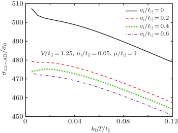
In Fig.
Finally, we study the effect of the chemical potential on the impurity potential strength dependence of the electrical conductivity of the AB stacked bilayer graphene, and the main results are presented in Fig.
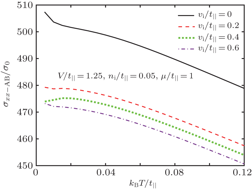 | Fig. 8. Normalized electrical conductivity σxx/σ0 of biased doped AB stacked bilayer graphene as a function of temperature kBT/t∥ for different scattering strengths vi/t∥ for ni = 0.05. The normalized bias voltage is assumed to be V/t∥ = 1.25. |
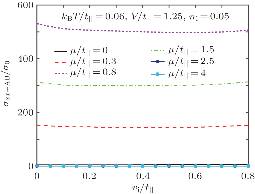 | Fig. 9. Normalized electrical conductivity σxx/σ0 of biased doped AB stacked bilayer graphene as a function of normalized scattering strength vi/t∥ for different chemical potentials μ/t∥ for ni = 0.05. The normalized temperature is assumed to be kBT/t∥ = 0.06. |
We have presented the electrical conductivity of both simple and bernal stacked biased bilayer graphene in the presence of impurity atoms. With the tight binding model Hamiltonian including a local energy term, the electronic excitation spectrum has been studied. Using the self-consistent Born approximation and the linear response theory, the electrical conductivity of disordered bilayer graphene has been obtained. Specially, the effects of the impurity concentration and the scattering strength on the temperature dependence of conductivity have been investigated. We find that the electrical conductivity decreases with increasing impurity concentration for all values of scattering potential strength. The results also show that there is a peak in the electrical conductivity in terms of temperature for all scattering strengths.
| 1 | |
| 2 | |
| 3 | |
| 4 | |
| 5 | |
| 6 | |
| 7 | |
| 8 | |
| 9 | |
| 10 | |
| 11 | |
| 12 | |
| 13 | |
| 14 | |
| 15 | |
| 16 | |
| 17 | |
| 18 | |
| 19 | |
| 20 | |
| 21 | |
| 22 | |
| 23 | |
| 24 | |
| 25 | |
| 26 | |
| 27 | |
| 28 | |
| 29 | |
| 30 | |
| 31 | |
| 32 | |
| 33 | |
| 34 | |
| 35 | |
| 36 | |
| 37 | |
| 38 | |
| 39 | |
| 40 | |
| 41 | |
| 42 | |
| 43 | |
| 44 | |
| 45 | |
| 46 | |
| 47 | |
| 48 | |
| 49 | |
| 50 | |
| 51 | |
| 52 | |
| 53 | |
| 54 | |
| 55 | |
| 56 | |
| 57 | |
| 58 | |
| 59 | |
| 60 | |
| 61 | |
| 62 |