

Numerical simulation study of organic nonvolatile memory with polysilicon floating gate
[Yan Zhao-wen, Wang Jiao, Qiao Jian-li, Chen Wen-jie, Yang Pan, Xiao Tong, Yang Jian-hong†,  ]
]
]
|
|


† Corresponding author. E-mail:
A polysilicon-based organic nonvolatile floating-gate memory device with a bottom-gate top-contact configuration is investigated, in which polysilicon is sandwiched between oxide layers as a floating gate. Simulations for the electrical characteristics of the polysilicon floating gate-based memory device are performed. The shifted transfer characteristics and corresponding charge trapping mechanisms during programing and erasing (P/E) operations at various P/E voltages are discussed. The simulated results show that present memory exhibits a large memory window of 57.5 V, and a high read current on/off ratio of ≈ 103. Compared with the reported experimental results, these simulated results indicate that the polysilicon floating gate based memory device demonstrates remarkable memory effects, which shows great promise in device designing and practical application.
Organic nonvolatile floating gate memory (ONFGM) devices based on organic thin film transistors (OTFTs) with typical physical structures and unique working mechanism have been widely investigated recently due to their nondestructive read-out, simple preparation process and single transistor realization.[1–4] Meanwhile the performance of the ONFGM device was greatly improved by optimizing the physical structures and memory materials.[5,6] Relevant researches have demonstrated that high k dielectric materials because of their excellent capacitance ratio usually served as the gate dielectric layer to scale down operating voltage, and metallic nanoparticles were imbedded within the gate dielectric interface acting as charge trapping sites to reduce the stress-induced leakage current by precisely controlling the size and trap density of metallic nanoparticles.[7–12] It has also been demonstrated that memory performances could be improved with light assisted program.[13] Recently, Yi et al. demonstrated that light illumination and electrical stress can act as an independent programming/erasing operation method, by which the stable ambipolar memory properties were observed and a large memory window, excellent retention time and high ON/OFF current ratio of the ambipolar memory device were obtained to be 70 V, 104 s and 104, respectively.[14] Tseng et al. improved the characteristics of the memory device, and their researches mainly focused on introducing a double-floating gate monolayer, which included a diacetylenic (DA) unit as a hole carrier trap and a naphthalenetetracarboxyldiimide (ND) unit as an electron carrier trap.[15] The memory device with the double-floating gate monolayer exhibited a larger memory window, longer retention time and rather stable device characteristics than with the single-floating gate. Kim et al. placed a graphene oxide layer between two polystyrene (PS) layers as charge storage medium, and their work demonstrated the multilevel characteristics of nonvolatile floating-gate memory devices.[16] In addition, Jung et al. investigated the particle size effects on the memory performance by using semiconducting cobalt ferrite nanoparticles as charge trap sites.[17] Nevertheless, up to now it has remained a significant challenge of improving the data retention property and scale down operating voltage of ONFGM devices, simultaneously. Clearly, the memory effects are strongly dependent on the floating gate trapping and detrapping charge carriers at an external gate voltage. It is actually difficult to measure the variations of charge stored in a floating gate in the P/E process. While research about multilevel characteristics of the ONFGM device with a sandwiched poly-silicon (Poly-Si) floating gate between two oxide layers, in particular the variations of charge stored in the floating gate, have been scarce. Hence, it is highly needed to have an insight into the operating mechanism and the shifted effects of transfer curves at different programming and erasing voltages (VP/VE).
In this work, simulation for the electrical characteristics of the ONFGM device is developed by employing poly-Si as a floating gate. Because poly-Si has widely been studied in inorganic memory devices and the relevant results show that poly-Si effectively increases charge traps.[18] In particular, the shifted effects of transfer curves and the corresponding variations of charge stored in the floating gate during P/E operations are discussed in detail by the simulated results and the energy band diagrams. In addition, simulation on dynamic memory switching behavior is also carried out.
The rest of the present paper is organized as follows. In Section 2, the device structure and relevant simulating models are introduced. The numerical simulation process is also given. In Section 3, the numerical simulation for the electrical characteristics including output and transfer curves and memory features of ONFGM are discussed in detail. Finally, some significant conclusions are drawn from the present studies in Section 4.
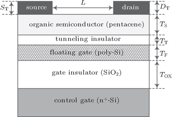
Taking into consideration the sequence of thermal treatment process and the excellent performance the memory exhibits, the configuration of device in this work is designed into bottom-gate, top-contact p-channel ONFGM as shown in Fig.
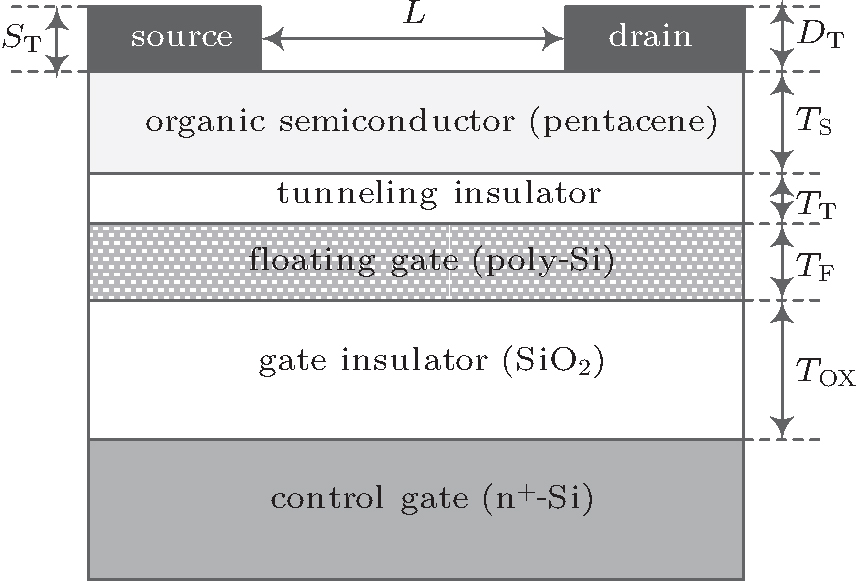 | Fig. 1. Schematic cross section of ONFGM based on pentacene with a bottom-gate, top-contact structure. |
| Table 1. Physical and structural parameters used for device simulation. . |
The geometry of the ONFGM device resembles that of OTFT except the tunneling insulator and floating gate that are sandwiched between the organic semiconductor and the gate insulator. Based on the investigation of p-channel OTFTs,[21,22] the charge carriers transporting mechanism is strongly dependent on the temperature, electric field and holes traps between the organic semiconductor channel, electrode and gate dielectric layer.[23,24] Therefore, the simulations for the charge carrier transport of the ONFGM device are carried out by solving Poisson’s equation, continuity equation and holes drift-diffusion equation, which are described as follows:[25–28]


In this model, μp0 is the low field mobility and Eh0 represent the activation energy for hole (E = 0) which is equal to 0.018 eV, β is the hole Poole–Frenkel factor, and γ is the fitting parameter. For obtaining prominent simulation results, the contact between electrode and organic semiconductor are regarded as a Schottky barrier (0.1 eV ∼ 0.3 eV). Moreover, in an organic semiconductor material, the effective density of states at the lowest unoccupied molecular orbital (LUMO) level is considered to be the same as that at the highest occupied molecular orbital (HOMO) level.[30,31] In addition, the hot carrier injection and Fowler–Nordheim (FN) tunneling model are utilized for simulating holes injected into or extracted from the floating gate during P/E operation. The thermal emission current J and tunneling current JFN are respectively given as follows:[32,33]


Based on the models above, the electrical characteristics of the ONFGM device are simulated and calculated reasonably through Newton’s iteration method. Figure
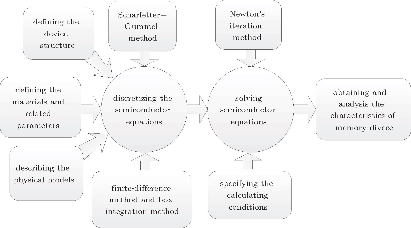 | Fig. 2. Flow chart of numerical simulation. |
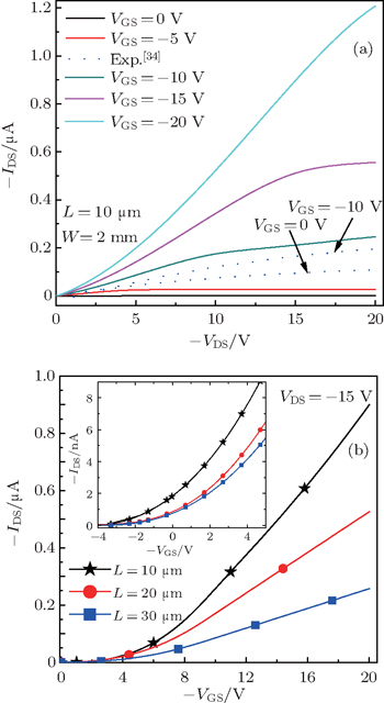
The simulations of the output and transfer characteristics of our present ONFGM device are performed, and the simulated results indicate that the device features typical p-channel field-effect behavior in hole-accumulation mode during VDS ranging from 0 V to −20 V and VGS from 0 V to −20 V in steps of −5 V as shown in Fig.
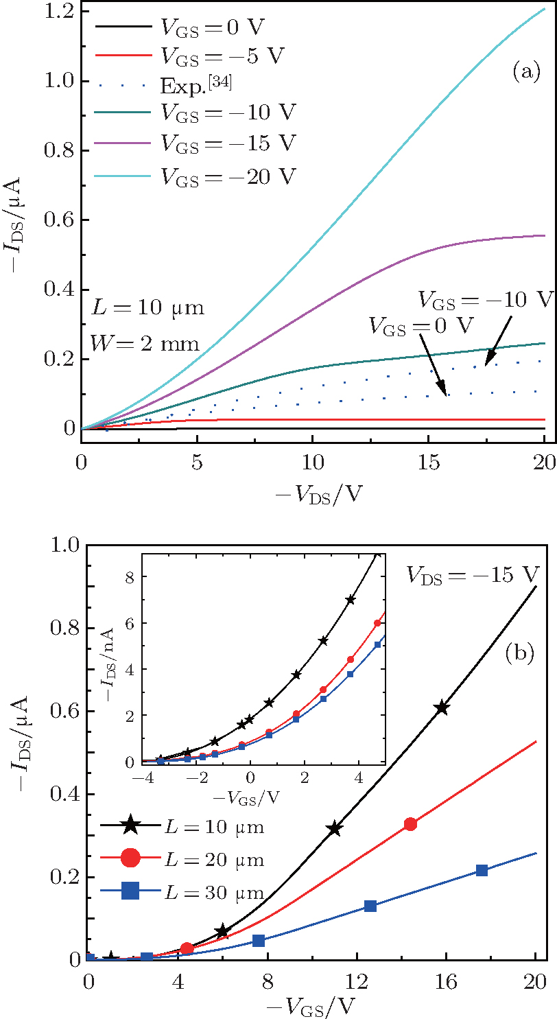 | Fig. 3. (a) Output characteristic curves of ONFGM with a channel length of 10 μm. (b) Comparison of the transfer characteristic curves with different channel lengths. The inset shows the transfer curves at low gate voltages. |
According to the above analysis, by employing the hot hole injection model and the FN tunneling model, the (P/E) characteristics of the present ONFGM are simulated and the effects associated with shifts in transfer curves are examined through a series of P/E operations in a sequence of programing voltages (VP) and erasing voltages (VE), respectively. For all of the P/E operations, the drain-source voltage (VDS) is maintained at 0 V and the P/E time is set to be 5 s, holes are majority charge carriers in the present ONFGM which is operated in the p-channel as mentioned in Subsection 3.1.
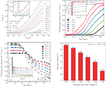
Figure
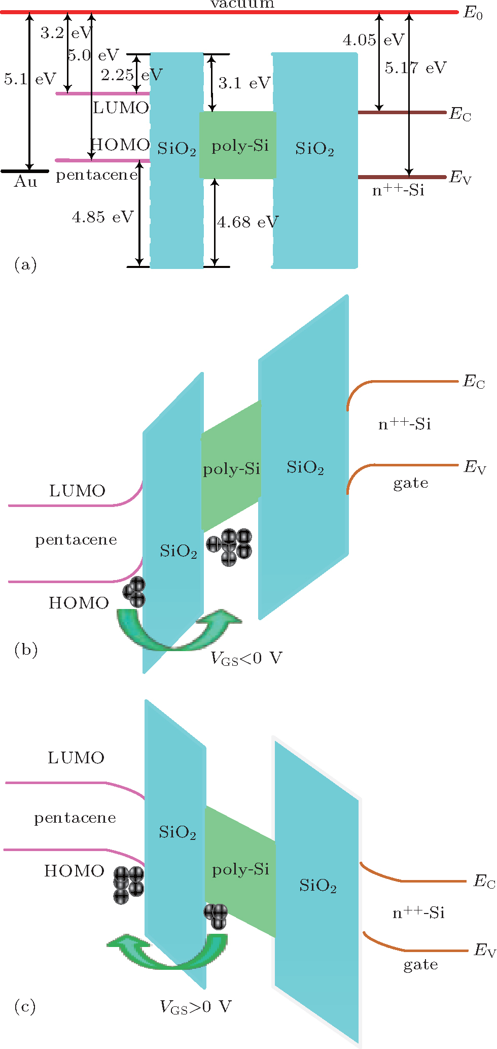 | Fig. 4. (a) Energy level diagram of ONFGM without applying voltage, (b) energy band diagrams of ONFGM during programming, and (c) erasing operations. |
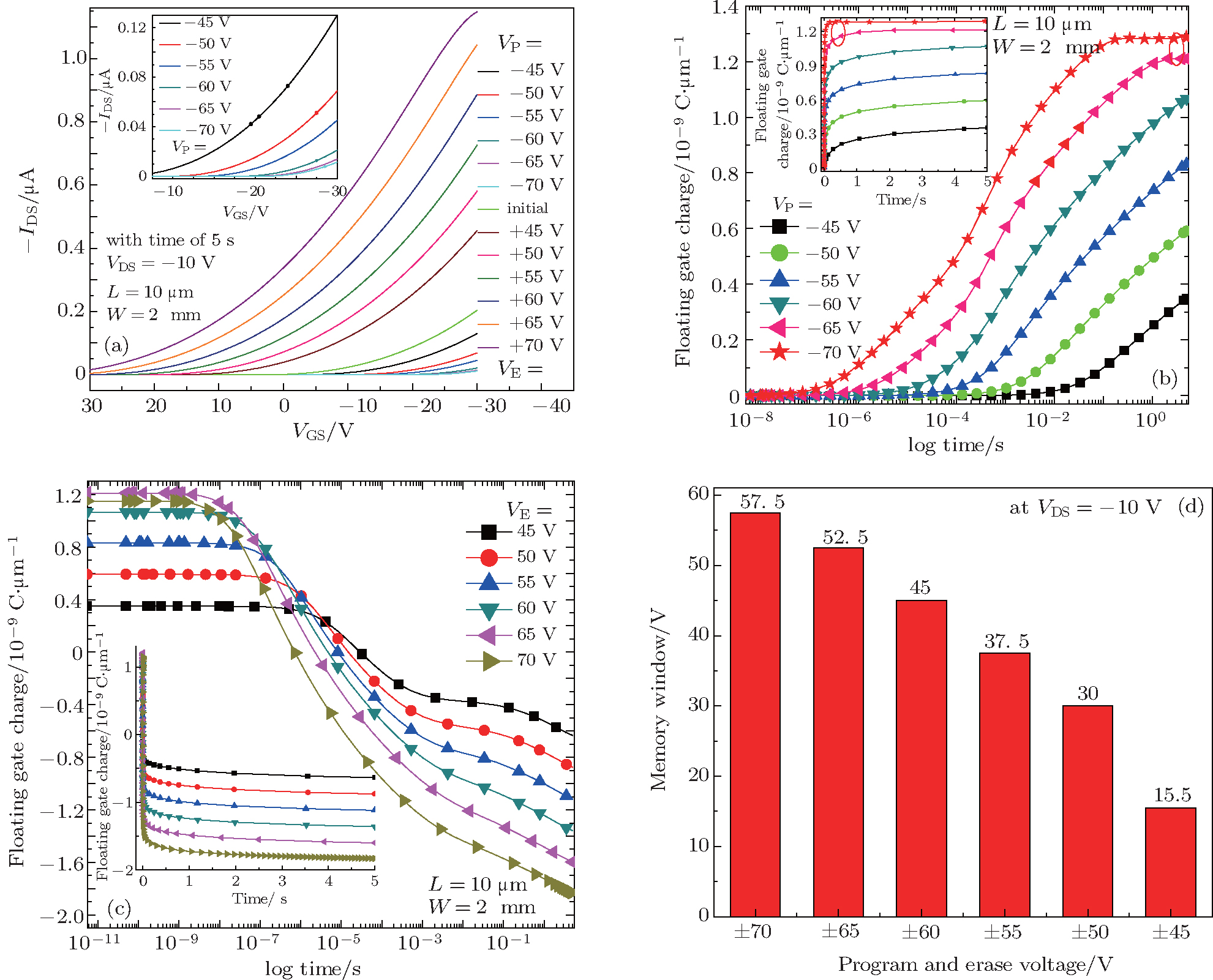 | Fig. 5. (a) Transfer curves of the ONFGM device in the initial and a series of post-P/E operations at various of VP/VE voltages in a time of 5 s. The inset shows the shifts in transfer curves during P operations at VGS ranging from −5 V to −30 V. (b) Corresponding variations of charge stored in the poly-Si floating gate in logarithmic coordinates and the inset in linear coordinates during P operation and (c) E operation. (d) Memory windows for various VP and VE voltages. |
It is clearly revealed that the transfer curves shift rapidly in the negative direction with the increase of VP from −45 V to −60 V, and then more slowly as VP increases from −60 V to −70 V. To further confirm that the shift effect of the transfer curve is attributed to the trapped holes in the floating gate, the variations of poly-Si floating gate charge are simulated as shown in Fig.
After a series of programing operations, a series of erasing operations are performed. As depicted in Fig.
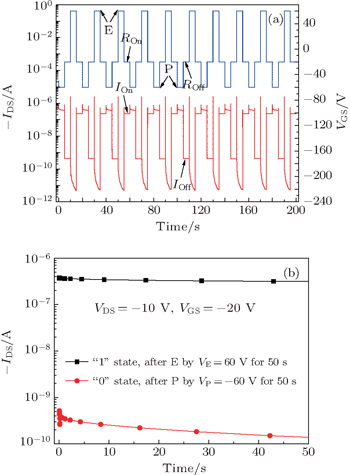
In the present ONFGM device, the drain current responses for program, read, erase, and read cycles, which are called dynamic memory switching behaviors, are also simulated at sequential and repeated gate voltages of −60, −20, 60, and −20 V in an interval time of 5 s as shown in Fig.
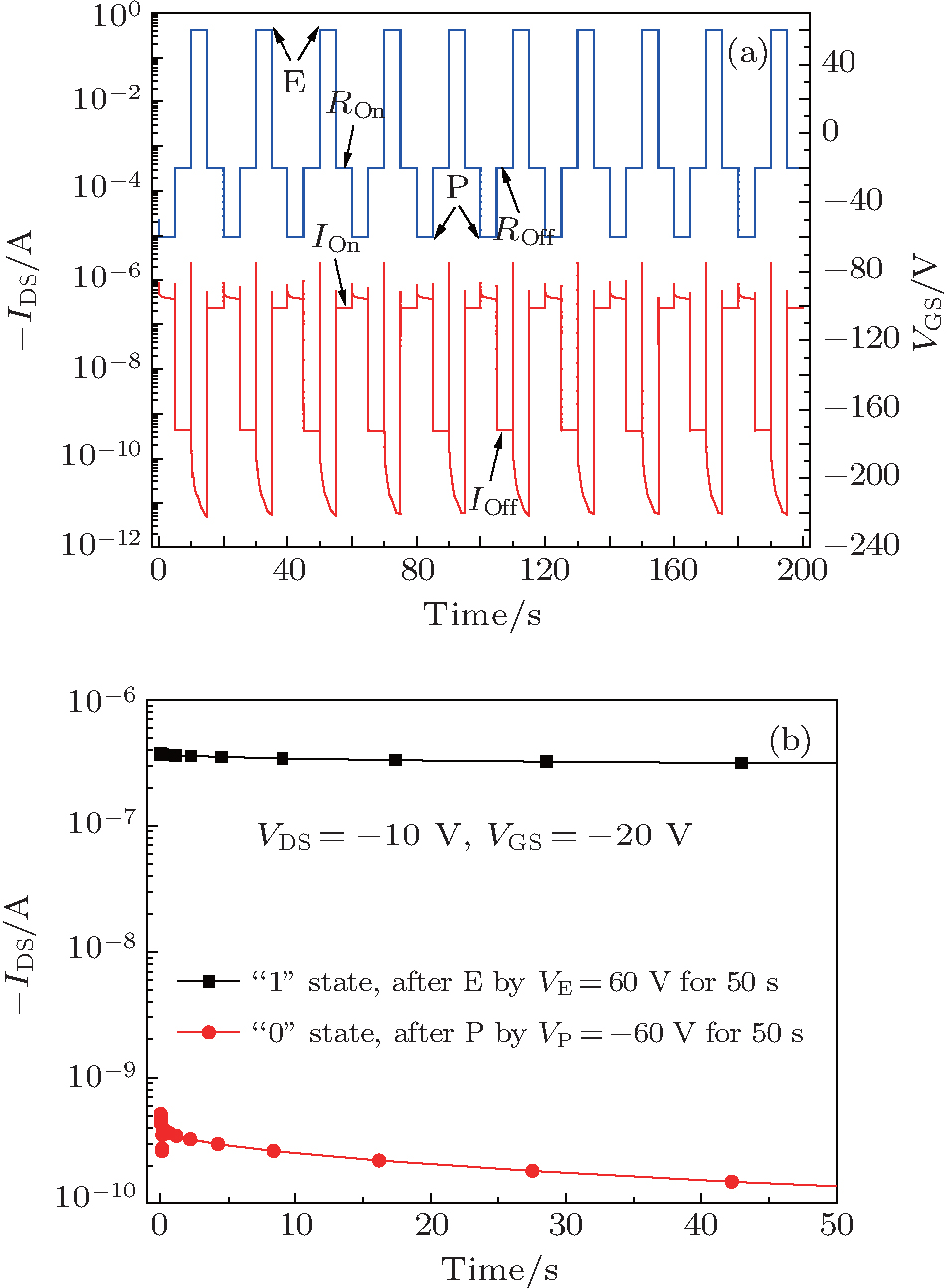 | Fig. 6. (a) Switching behavior for the ONFGM device with poly-Si floating gate (E: erase, P: program, ROn: read-on state, and ROff: read-off state), and (b) the drain currents of ON state and OFF state after erase and program. |
In this work, simulations for the present ONFGM device by sandwiching polysilicon between oxide layers as a floating gate are performed through basic organic transporting, hot holes injection, and FN tunneling models. The simulated results demonstrate that the poly-Si floating gate based ONFGM device exhibits remarkably memory effects which include a large memory window of 57.5 V, excellent switching behavior, and a high read IOn/IOff of ≈ 103. In addition, the values of shifts in transfer curves towards the positive direction after erasing operations are larger than towards the negative direction after programing operations. It is of great value that employing the simulations for the variations of charge stored in the floating gate during P/E operations examines and explains the shifted effects of transfer curves which are attributed to the transferred charge carriers at various VP/VE voltages. These simulated results are significantly helpful in designing devices and understanding the storage characteristics of the ONFGM device.
| 1 | |
| 2 | |
| 3 | |
| 4 | |
| 5 | |
| 6 | |
| 7 | |
| 8 | |
| 9 | |
| 10 | |
| 11 | |
| 12 | |
| 13 | |
| 14 | |
| 15 | |
| 16 | |
| 17 | |
| 18 | |
| 19 | |
| 20 | |
| 21 | |
| 22 | |
| 23 | |
| 24 | |
| 25 | |
| 26 | |
| 27 | |
| 28 | |
| 29 | |
| 30 | |
| 31 | |
| 32 | |
| 33 | |
| 34 | |
| 35 | |
| 36 | |
| 37 | |
| 38 | |
| 39 |