High-speed waveguide-integrated Ge/Si avalanche photodetector
Cong Hui, Xue Chunlai†, , Liu Zhi, Li Chuanbo, Cheng Buwen, Wang Qiming
State Key Laboratory on Integrated Optoelectronics, Institute of Semiconductors, Chinese Academy of Sciences, Beijing 100083, China


† Corresponding author. E-mail: clxue@semi.ac.cn

Project supported by the National State Basic Research Program of China (Grant No. 2013CB632103) and the National Natural Science Foundation of China (Grant Nos. 61177038, 61377045, and 61176013).

Abstract
Abstract

Waveguide-integrated Ge/Si heterostructure avalanche photodetectors (APDs) were designed and fabricated using a CMOS-compatible process on 8-inch SOI substrate. The structure of the APD was designed as separate-absorption-charge-multiplication (SACM) using germanium and silicon as absorption region and multiplication region, respectively. The breakdown voltage (Vb) of such a device is 19 V at reverse bias and dark current appears to be 0.71 μA at 90% of the Vb. The device with a 10-μm length and 7-μm width of Ge layer shows a maximum 3-dB bandwidth of 17.8 GHz at the wavelength of 1550 nm. For the device with a 30-μm-length Ge region, gain-bandwidth product achieves 325 GHz.

1. Introduction

Avalanche photodetectors (APDs) are widely used in fiber-optic communications due to their internal carrier multiplication mechanism.[1,2] The applications of conventional III–V compound semiconductor APDs are limited because of their low gain-bandwidth products.[35] Their typical values are in the range of 100–150 GHz, which make them less attractive for high-speed communication. Silicon (Si) is considered the best material for the multiplication layer in an APD in contrast to other bulk semiconductors because of its low ratio of the ionization coefficients of electrons and holes (0.01–0.1).[6,7] In addition, compared with other semiconductors, Si shows a very low temperature dependence on the avalanche breakdown.[8] Thus Ge/Si APDs with separated-absorption-charge-multiplication (SACM) structure have become greatly promising for high response and high speed at 1550 nm wavelength.[9,10] Using germanium and silicon as absorption and multiplication layer respectively, could effectively avoid the carrier feedback loops caused by carrier multiplication in the absorbing region.[11] The fact that Ge has similar crystal structure and material characteristics to Si makes the design and manufacture of APDs compatible with the existing CMOS process technology. The above advantages could achieve properties of high gain-bandwidth products, low noise, temperature independence and low cost for APDs. Recent advancement reveals that group-IV materials could be promising candidates for manufacturing high-performance APDs. The first Si-waveguide-integrated Ge/Si APD was fabricated by Zhu et al., which has a responsivity of 7.2 A/W at 1550 nm with a 3-dB bandwidth of 3.3 GHz.[12] Kang et al. have demonstrated a top illuminated Ge/Si APD with a quite high gain-bandwidth product of 340 GHz and a sensitivity of −28 dBm at a photon wavelength of 1310 nm.[13]

In this paper, we demonstrate waveguide-integrated Ge/Si SACM APDs with selective epitaxial growth germanium and silicon waveguide on 8-inch SOI substrate.[14] A step-coupler was designed for high efficient vertical coupling between Si waveguide and Ge/Si APD.[15] The crystal quality of the epi-Ge absorption layer is better than that of non-selective growth. These features ensure that such an APD has a very low dark current and high optical absorption. We designed and fabricated the waveguide-integrated Ge/Si APD in order to further improve both speed and responsivity with a smaller area of depletion capacitance and longer germanium absorption region than vertical incidence APD.[16]

2. Device fabrication

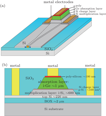
Waveguide-integrated Ge/Si avalanche photodetector design features a separate-absorption-charge-multiplication (SACM) configuration in which germanium and silicon were employed for light absorption and carrier multiplication, respectively. The device fabrication was started from an 8-inch Si-on-insulator (SOI) substrate with a 220-nm-thick silicon top layer and a 2-μm-thick buried oxide. Channel waveguide with a taper width of 180 nm was first formed for light guidance and electrical isolation, and the taper was designed to improve the efficiency of coupling light to the optical fiber. Ion implantation of arsenic dopants was performed to form the bottom n-type layer, followed by high-dose phosphorus implantation to form a good n-type Ohmic contact. A 10-nm-thick oxide window was formed for selective Si epitaxy. The epi-Si layer with a thickness of 700 nm was grown using an ultra-high vacuum chemical vapor deposition (UHVCVD) reactor, which was followed by boron implantation to form a p-type charge layer. After the formation of another oxide window, a 1-μm-thick hetero-epitaxy Ge layer was selectively grown using the same UHVCVD reactor. Then a 100-nm-thick poly silicon was deposited and followed by a high dose of boron ion implantation. The dopants were activated at 750 °C for 3 minutes in the atmosphere of nitrogen to form a good p-type Ohmic contact. Finally a 1.5-μm-thick TaN/Al was deposited and metalized.

The schematic configuration of an evanescently coupled waveguide APD is shown in Fig. 1(a). Light propagating through the silicon optical waveguide will be coupled evanescently to the germanium layer and will be absorbed. Figure 1(b) shows the schematic configuration of an SACM Ge/Si APD, which consists of 1-μm-thick Ge absorption layer, 100-nm-thick Si charge layer, and 600-nm-thick Si multiplication layer. A coplanar waveguide (CPW) transmission line with characteristic impedance of 50 Ω was fabricated for high-speed measurement probe.

Fig. 1. (a) The schematic configuration of an evanescently coupled waveguide APD; (b) the schematic configuration of an SACM Ge/Si APD.
3. Device characteristics and discussion

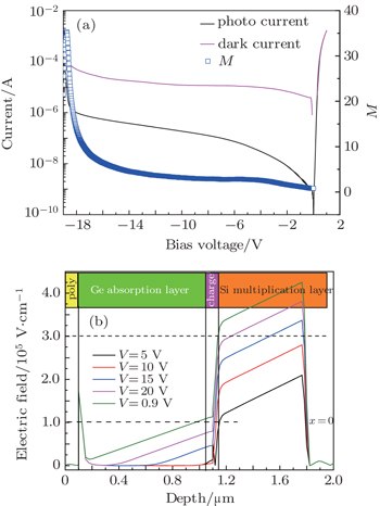
The measured dark current and photocurrent of a typical 10-μm-length device at room temperature are shown in Fig. 2(a), which were measured with an Agilent B1500 semiconductor device analyzer and a laser of wavelength of 1550 nm. All tested devices exhibited typical current–voltage characteristics of SACM APDs, with clear rectifying behaviors. The measured avalanche breakdown voltage Vb (defined at a dark current of 100 μA) for the device is 19 V at reverse bias. The dark current is 0.71 μA at a bias that is equal to 90% of the breakdown voltage. The dark current is comparable to the typical Si/Ge PIN PDs.

Fig. 2. (a) Measured dark current (black curve) at room temperature, total photocurrent (red curve) under 1550-nm illumination and multiplication gain factor (M) (dashed curve) versus bias voltage of a Ge/Si APD with 10-μm-length and 7-μm-width germanium absorption layer; (b) simulation results of the electric field distribution in the device layer.

When the bias is less than punch-through voltage, the depletion region is solely confined in the silicon region. The dark current from simulation is flat and in the sub-nA level, the measured dark current is much larger than the level. The main reason is the quality of the epitaxial silicon layer. In the Ge absorption region, incident photons are absorbed and photocarriers generated. Under reverse bias, the holes are swept toward the p+ contact and electrons toward the n+ contact. When traveling in the Si multiplication region with a high electric field, electrons primarily undergo a series of impact ionizations, creating more electron–hole pairs, which consequently amplifies photocurrent.

The electric field distribution was calculated along the longitudinal cross section of a waveguide-integrated Ge/Si APD. Figure 2(b) shows the device simulation results of the electric field distribution in the device layers. From the perspective of the high-sensitivity and high-speed APD design, the internal electric field distribution must meet the following basic requirements. Firstly, photon-generated carriers in Ge absorption layer should drift at the speed of their saturation velocity (5 × 106 cm/s) so as to minimize transit-time and should avoid avalanche multiplication process. So the electric field within this region should be kept above 3 kV/cm and below 100 kV/cm. Secondly, the doping concentration in the charge layer should be accurately designed to achieve the expected electric field distribution. The applied electric field of Si multiplication region should be higher than 300 kV/cm to ensure that the carriers multiplication process could be built up through impact ionization.

In order to characterize the optical response, a single-mode lensed fiber was used for injecting light at a wavelength of 1550 nm into the Si waveguide. The primary responsivity was measured using a conventional waveguide-integrated Ge/Si p–i–i–n detector with the same geometric structure, and the measured result is 0.8 A/W. By normalizing the measured APD’s responsivity to the primary responsivity of the reference detector, the multiplication (M) gain factor can be calculated. In Fig. 2(a), the measured results show that M could reach a value as high as 10 when operated at 90% of the breakdown voltage. The multiplication factor enhances with the increase of reverse bias because of the avalanche multiplication effect. Further increasing the applied bias causes a rapid rising in photo current. Then the M factor begins to decrease as the bias continues increasing which is due to the reason that the electrical field of the multiplication region decreases, and thus cannot support for such a high avalanche multiplication process. Figure 3 shows the M factors of devices with different lengths of Ge layer, 10 μm, 30 μm, and 50 μm. The maximum M factor is 53 for the device with 30-μm-length absorption region, whereas the device with 50-μm-length Ge layer has a poor multiplication factor of 16, which is much lower than that of 10-μm-length device. As the length of germanium region increases, optical absorption could achieve a state of saturation, so no more carriers would generate. However, as shown in the inset figure, devices with longer Ge region also show higher dark currents, arising from more dislocations. This leads to the recombination of photon-generated carriers and, thus, reduces optical response.
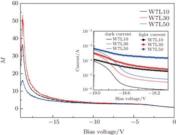
Fig. 3. Multiplication factors M of devices with different lengths of Ge layer; inset figure shows dark and light currents of these devices before break-down.

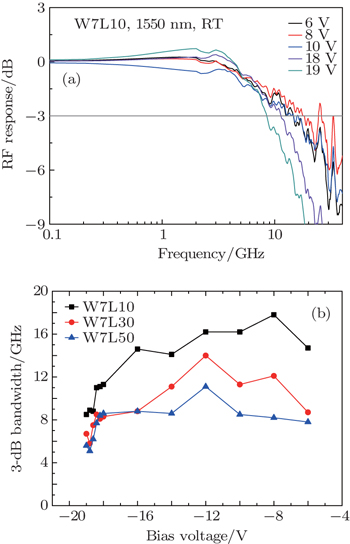
The electrical 3-dB-bandwidth of the waveguide-integrated Ge/Si APD was measured using a Yenista tunable laser, Sumitomo Osaka cement 40 Gbps intensity modulator and an Anritus Vector Network Analyzer at 1550 nm. Figure 4(a) plots the normalized radio frequency (RF) responses for device with 10-μm-length and 7-μm-width epi-Ge layer at five different reverse biases, 6 V, 8 V, 10 V, 18 V, and 19 V, which are 14.7 GHz, 17.8 GHz, 16.2 GHz, 11.3 GHz, and 8.5 GHz, respectively. Figure 4(b) shows 3-dB-bandwidth of devices with different Ge-layer geometric constructions under reverse bias. RF response is limited by RC delay, transit time constant, and avalanche multiplication process built-up time. An APD can be approximated as a series of two pn junctions. For each junction, the barrier capacitance can be calculated by the following equation:

Fig. 4. (a) RF response for APD with 10-μm-length Ge layer at reverse bias of 6 V, 8 V, 10 V, 18 V, and 19 V; (b) 3-dB-bandwidth versus bias voltage for devices with different lengths of Ge layer.

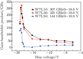
In Eq. (1), ε0 is permittivity of vacuum, εr is the relative permittivity of junction material, A is the area of junction, N1 and N2 are concentrations of each side of junction, VD is barrier potential difference, and V is the bias voltage of junction. For a device with certain structure, CT is inversely proportional to the applied voltage. At low reverse bias, the junction barrier capacitance keeps in a large value, so RC delay plays a major role in limitation of the RF response. With the increase of reverse voltage, barrier capacitance decreases. RC delay achieves the minimum when the device is under punch-through voltage, at which both of the absorption and multiplication regions are completely depleted. As shown in Fig. 2(b), when the electric field is not high enough to make the carriers transit at their saturation velocity, transit time constant is another limitation factor for 3-dB-bandwidth. At higher bias voltage, the avalanche multiplication process starts building up so that the optical response improves with the increase of negative bias voltage. At the same time, the process pulls the frequency response to a quite low level. For devices with larger germanium area, capacitances are larger under the same bias voltage as well as the series resistances, so the devices with 10-μm-length Ge absorption layer show higher RF response than that of longer Ge region. The maximum 3-dB-bandwidth of devices with 10-μm-length, 30-μm-length, and 50 μm-length Ge layer are 17.8 GHz at −8 V, 14 GHz at −12 V and 11 GHz at −12 V, respectively. When the device shows a large 3-dB-bandwidth, the optical response cannot achieve a satisfactory level at low bias voltage. With the increase of reverse bias, avalanche multiplication process begins to build up followed by increasing the multiplication factor and reduction of the 3-dB-bandwidth. Figure 5 plots gain-bandwidth products of different devices against reverse bias voltage. The maximum values for waveguide-integrated APD with 10-μm, 30-μm, and 50-μm Ge layer are 307 GHz at −18.8 V, 325 GHz at −18.6 V, and 144 GHz at −18.8 V, respectively.

Fig. 5. Gain-bandwidth product against reverse bias voltage of different devices.
4. Conclusion

A waveguide-integrated Ge/Si avalanche photodetector (APD) featuring separate-absorption-charge-multiplication (SACM) was demonstrated using a CMOS-compatible process on 8-inch SOI platform. The device with a length of 30-μm Ge layer achieved a multiplication gain factor of 53 for a C-band communication wavelength of 1550 nm. The maximum 3-dB-bandwidth for the APD was 17.8 GHz at a reverse bias voltage of 8 V for the device with 10-μm-length Ge layer. By considering both optical and RF response, the largest gain-bandwidth product was 325 GHz for the device with 30-μm-length absorption region under a reverse bias of 18.6 V.

Reference
1Ang K WNg J WLim A E JYu M BLo G QKwong D L2010Optical Fiber Communication ConferenceMarch 21–25, 2010San Diego, California, United StatesJWA36
2Virot LCrozat PFedeli J MHartmann J MMarris-Morini DCassan EBoeuf FViven L2014Nat. Commun.54957
3Duan NLiow T YLim A E JDing LLo G Q 2012 Opt. Express 20 11031
4Rouvie ACarpentier DLagay NDecobert JPommereau FAchouche M 2008 IEEE Photon. Technol. Lett. 20 455
5Refaat T FAbedin M NSingh U N2005Conference on Lasers and Electro–OpticsMay 22Baltimore, Maryland, United StatesJThl6
6Webb P PMcIntyre R JConradi J1974RCA Rev.35234
7Kang YHuang ZSaado YCampbell JPauchard ABowers JPaniccia M2011Optical Fiber Communication ConferenceMarch 6–10, 2011Los Angeles, California, United StatesWOZ110.1364/OFC.2011.OWZ1
8Kang YZadka MLitski SSarid GMorse MPaniccia M JKuo Y HBowers JBeling ALiu H D 2008 Opt. Express 16 9365
9Huang M YShi TCai P FWang L BLi SChen WHong CPan D2014The European Conference on Optical Communication (ECOC)September 21–25, 2014Cannes, France
10Kang Yet al2009IEEE International Conference on Group IV PhotonicsSeptember 9–11, 2009San Francisco, CA, USA2510.1109/LPT.2008.918229
11Duan NLiow T YLim A EDing LLo G Q2013Optical Fiber Communication ConferenceMarch 17–21, 2013Anaheim, California, United StatesOM3K.310.1364/OFC.2013.OM3K.3
12Zhu SKah-Wee ARustagi S CWang JXiong Y ZLo G QKwong D L 2009 IEEE Electron. Dev. Lett. 30 934
13Kang Y Met al 2008 Nat. Photon. 3 59
14Kim MOlubuyide O OYoon J UHoye J L 2008 ECS Trans. 16 837
15Wang XLiu J 2011 IEEE Photon. Technol. Lett. 23 146
16Li CXue C LLi Y MLi C BCheng B WWang Q M2015Chin. Phys. B24038502