† Corresponding author. E-mail:
Project supported by the National Natural Science Foundation of China (Grant No. 61501091) and the Fundamental Research Funds for the Central Universities of Ministry of Education of China (Grant Nos. ZYGX2014J003 and ZYGX2013J020).
Design and characterization of a G-band (140–220 GHz) terahertz monolithic integrated circuit (TMIC) amplifier in eight-stage common-emitter topology are performed based on the 0.5-μm InGaAs/InP double heterojunction bipolar transistor (DHBT). An inverted microstrip line is implemented to avoid a parasitic mode between the ground plane and the InP substrate. The on-wafer measurement results show that peak gains are 20 dB at 140 GHz and more than 15-dB gain at 140–190 GHz respectively. The saturation output powers are −2.688 dBm at 210 GHz and −2.88 dBm at 220 GHz, respectively. It is the first report on an amplifier operating at the G-band based on 0.5-μm InP DHBT technology. Compared with the hybrid integrated circuit of vacuum electronic devices, the monolithic integrated circuit has the advantage of reliability and consistency. This TMIC demonstrates the feasibility of the 0.5-μm InGaAs/InP DHBT amplifier in G-band frequencies applications.
In the terahertz (0.1–10 THz) field, the vacuum electronic device (VED),[1] quantum cascade laser (QCL),[2–4] and solid state device[5,6] have received a great deal of attention. Benefiting from the robust performance, low operation voltage, room temperature operation and easy mass-production, the solid state devices have progressed very rapidly in the last several years. InP DHBT is a promising technology in the terahertz solid state device field.[7,8] Recently massive G-band (140–220 GHz) and H-band (220–325 GHz) amplifiers were presented based on 250-nm or 150-nm InP DHBT technology.[9–12] InP solid state devices show splendid prospects in imaging, radar, spectroscopy, and communication systems operating in the terahertz frequency band. Scaling the emitter length under 0.25 μm requires complex fabrication procedures such as e-beam lithography, refractory contact metal deposition, etc. Meanwhile, the 0.5-μm InGaAs/InP DHBT process just needs ordinary optical lithography, wet-etching and deposition technology. However, a larger emitter length leads to a lower cut-off frequency (ft) and a lower power gain in a terahertz band. Therefore, the critical problem of using the 0.5-μm processing in a terahertz band is the maximum utilization of the gain resource. A precise modeling and designing method should be utilized to achieve the goal. In this paper, we present a G-band amplifier based on the 0.5-μm InGaAs/InP DHBT process. The amplifier was designed in the University of Electronic Science and Technology of China (UESTC) and made in the Nanjing Electronic Devices Institute (NEDI). The amplifier was designed with a modified Agilent-HBT model and Keysight full-wave simulation software advance design system (ADS) momentum. Measurements demonstrate a more than 15-dB gain at 140–190 GHz and a peak gain of 20 dB at 140 GHz. The saturation output powers are −2.688 dBm at 210 GHz and −2.88 dBm at 220 GHz, respectively. This is the first report on an amplifier operating in the G-band based on 0.5-μm InP DHBT technology. This MMIC demonstrates the feasibility of 0.5-μm InGaAs/InP DHBT amplifiers operating at G-band frequencies.
The epitaxial layer of the DHBT is grown on a 3-inch semi-insulating InP substrate by using molecular-beam epitaxy (MBE). The layer structure is shown in Table
After material epitaxy, geometry is determined by using i-line stepper lithography. Ti/Pt/Au is used as the emitter contact. Three mesas are formed through selective wet-etching, and the etching time is accurately controlled to prevent over etching. The base contact metal is determined by using a self-aligned technique. Pt/Ti/Pt/Au is used as the base contact, for Pt can penetrate through the surface oxide layer of the InGaAs base, which is of benefit to achieving a low base contact resistivity.[15] All metals are formed through deposition and the lift-off technique. After metal posts and device isolation processes, BCB is used as a passivation and planarization layer. Finally, a metal pad is formed, and the device process is finished. DC characteristics are measured by using an Agilent semiconductor parameter analyzer as shown in Fig.
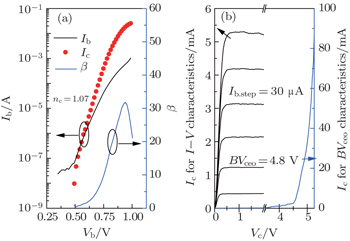 | Fig. 1. DC characteristics of the InGaAs/InP DHBT: (a) gammel plot Ib (left) and current gain β (right) at Vcb = 0 V; (b) I–V characteristics (left) and BVCEO measurement (right). |
| Table 1. Layer structure of the InGaAs/InP DHBT. . |
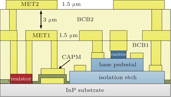
The area of the emitter contact is 0.5 μm×5 μm. Transmission line model (TLM) measurements show a base contact resistivity of ρbc = 3.9 Ω · μm2 and base sheet resistance of Rsh,b = 737 Ω/square, giving an estimated base resistance of 18.9 Ω. MMIC fabrication includes 2-levels of interconnect metal, metal 1 (MET1) and metal 2 (MET2), separated by 3.0-μm BCB (εr = 2.7). MIM capacitors (SiNx, 0.3 fF/μm2) are formed between the collector metal (CM) and capacitor metal (CAPM), and 250-Ω/square thin-film resistors (TFRes) are available. The cross section of this process is shown in Fig.
Two kinds of microstrip line are available in this process. The thin-film microstrip line (MET1 serves as the ground, and MET2 as the signal line), and inverted microstrip line (MET2 is used as the ground, and MET1 as the signal line).[16] The thin-film microstrip is close to the traditional microstrip, but the “ground” (MET1) floats on 620-μm InP substrate. In order to connect the MET1 ground to the real ground, bonding wire is necessary, which will introduce an inductive parasitic effect and deteriorates the chip performance. What is more, the large MET1 ground plane and thick InP substrate will generate a parasitic mode at high frequency such as dielectric waveguide mode or microstrip mode under MET1. On the contrary, the electromagnetic mode of the inverted microstrip is simple. No dielectric waveguide mode exists above the ground metal MET2, for the dielectric constant of air is much lower than those of the BCB and InP. The inverted microstrip configuration is convenient to the flip-chip package which requires no bonding wire, thus a large continuous ground plane is guaranteed. Therefore, the inverted microstrip has advantages in system level integration.[17]
DC-67 GHz measurements are carried out after performing an off-wafer line-reflect-reflect-match (LRRM) calibration on an Agilent N5247A programmable network analyzer (PNA). The pad frame parasitic parameters are de-embedded from the measured s-parameters by the open-short method. 75–110 GHz and 140–220 GHz RF device measurements are carried out after performing an on-wafer line-reflect-line (LRL) calibration, where the two ports reference planes after calibration are set to be at the edge of the device. The on-wafer calibration kit is designed and fabricated on InP wafer.
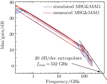
The large signal model we proposed in Ref. [18] is utilized here for device modeling and designing. Based on the Agilent-HBT model, the DC current function is modified to correct the heterojunction effect. The current gain β is simulated more precisely in the low current region. An RF current branch is added into an equivalent circuit to fit the non-thermal dispersion effect. The Agilent HBT model parameters are extracted from measurements at DC −67 GHz, and slightly adjusted according to high frequency measurements. The fitting results of max stable gain and max available gain (MSG&MAG) of HBT are shown in Fig.
The design presented in this paper uses an inverted microstrip line. The inverse microstrip simulated loss is 3.5 dB/mm at 300 GHz. The realizable characteristic impedances range from approximately 11.5 Ω to 53.2 Ω with signal line widths ranging from 3 μm to 30 μm.
The amplifiers are primarily optimized for high gain with adequate match between input and output. Under the simultaneous match condition, the optimum source impedance and load impedance can be calculated to be Zsource = 9.2 + j3.6 Ω, Zload = 12.5 + j44.3 Ω respectively. The matching networks are designed to obtain complex conjugate match of the input and output impedances of the device over a wide band width. To achieve a sufficient amount of gain, eight stages of HBT are cascaded. Inter-stage match also takes a complex conjugate match design. A 96-fF MIM capacitor for DC-blocking is inserted between stages. The capacitor and its parasitic effect are taken into account as a part of the matching network. The schematic is shown in Fig.
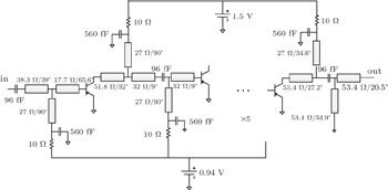 | Fig. 4. Schematic of the eight-stage amplifier. The electric length and characteristic impedance are calculated at 220 GHz. |
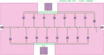
The DC bias is supplied through a long stub with a 560 fF decoupling capacitor. A 10 Ω series resistor is utilized to suppress low-frequency oscillation. All bias lines for the eight stages are tied together to minimize dc bond pads. The layout of the circuit is shown in Fig.
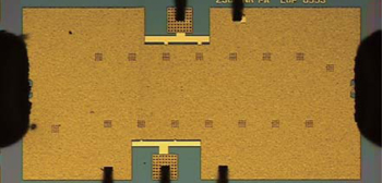
The amplifier MMIC is first tested by using the cascade probe station, WR-5 waveguide RF probes, DC probe, and WR-5 waveguide frequency extenders. The chip optical micrograph is shown in Fig.
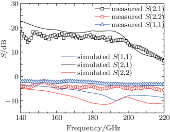
The small-signal measurements are performed with Vc = 1.5 V, Ic = 80 mA and Vb = 0.94 V, Ib = 3.2 mA. Small-signal measurements indicate a flat gain feature with more than 15 dB at the 140–190 GHz band. At 220 GHz, the amplifier still has 6.72-dB gain. The 3-dB band width of gain is 140–200.5 GHz. Figure
Next, output power is measured by using the setup shown in Fig.
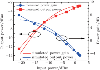
The output measurement results can be found in Figs.
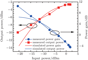 | Fig. 9. Simulated (line) and measured (dotted line) power gain and output power of the amplifier at 210 GHz. |
In this work, a G-band terahertz monolithic integrated amplifier is designed and fabricated based on 0.5-μm InP DHBT technology. The measured results show a flat gain feature with more than 15 dB at the 140–190 GHz band. The 3-dB band width of gain is 140–200.5 GHz. The saturation output powers are −2.688 dBm at 210 GHz and −2.88 dBm at 220 GHz respectively. Benefiting from the robust performance, low operation voltage, room temperature operation and easy mass-production, the solid state TMIC amplifier is suitable for driving an amplifier or a first stage small signal amplifier of the terahertz transceiver front end. The simulated and measured results show a similar trend while some deviation is also observed. A more precise modeling method of the terahertz device should be developed, and the statics model is important for the tolerant analysis. High-efficiency terahertz on-chip power combining technology is also important for the development of future solid state high-power devices.
| 1 | |
| 2 | |
| 3 | |
| 4 | |
| 5 | |
| 6 | |
| 7 | |
| 8 | |
| 9 | |
| 10 | |
| 11 | |
| 12 | |
| 13 | |
| 14 | |
| 15 | |
| 16 | |
| 17 | |
| 18 |


