Charge recombination mechanism to explain the negative capacitance in dye-sensitized solar cells
Feng Lie-Feng†, , Zhao Kun, Dai Hai-Tao, Wang Shu-Guo, Sun Xiao-Wei
Tianjin Key Laboratory of Low Dimensional Materials Physics and Preparing Technology, Faculty of Science, Tianjin University, Tianjin 300072, China


† Corresponding author. E-mail: fengliefeng@tju.edu.cn

Project supported by the National Natural Science Foundation of China (Grant Nos. 11204209 and 60876035) and the Natural Science Foundation of Tianjin City, China (Grant No. 13JCZDJC32800).

Abstract
Abstract

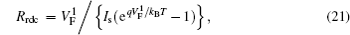
Negative capacitance (NC) in dye-sensitized solar cells (DSCs) has been confirmed experimentally. In this work, the recombination behavior of carriers in DSC with semiconductor interface as a carrier’s transport layer is explored theoretically in detail. Analytical results indicate that the recombination behavior of carriers could contribute to the NC of DSCs under small signal perturbation. Using this recombination capacitance we propose a novel equivalent circuit to completely explain the negative terminal capacitance. Further analysis based on the recombination complex impedance show that the NC is inversely proportional to frequency. In addition, analytical recombination resistance is composed by the alternating current (AC) recombination resistance (Rrac) and the direct current (DC) recombination resistance (Rrdc), which are caused by small-signal perturbation and the DC bias voltage, respectively. Both of two parts will decrease with increasing bias voltage.

1. Introduction

Dye-sensitized solar cells (DSCs) based on nanostructures have attracted significant attention in the research for an alternative and low-cost energy source, display items, and many other fields. Therefore, their optical and electrical characteristics have significant research value.[17] In the measurements of their properties, the impedance spectroscopy (IS) technique is one of the most effective methods and has been successfully widely applied in all kinds of solar cells, such as dye-sensitized solar cells (DSC), quantum dot-sensitized solar cells, extremely thin absorber solar cells, and organic solar cells.[1,3,4] Among alternative-current (AC) experimental features, an abnormally negative capacitance (NC) has been observed in many DSCs, which caused researchers’ great interest because of lack of a proper interpretation.[4] In addition, the NC has also been observed in many kinds of organic and inorganic electronic and optoelectronic devices, such as organic and inorganic LEDs.[4,814] In these papers, NC was proved as the internal behavior feature rather than being caused by measurement instruments. Therefore, it will affect the correct design of device’s model in the solar cells, as well as the accurate analysis of the operation mechanism of the photovoltaic devices.

Although the NC is in conflict with the well-known Shockley’s theory and model, and it is very difficult to be explained quantitatively, NC could be often explained with the aid of simulation tools based on complex device models in consideration of the particular system or structure of devices. In the latest developments, nanostructured DSC devices, NC still remains a major problem in device physics because the physical mechanism of NC in different devices should be very different.[1518] In a number of explanations, recombination and the associated model may be the most convincing.[18] In these models, the recombination process of carriers is separately considered, and NC is obtained from the impedance analysis of the equivalent circuit. However, the analytic explanation of NC from the physical mechanism rather than from the simple equivalent circuit could help us to understand the operation mechanisms of DSCs in depth, which will pave the way to design the reasonable equivalent circuit to further improve the performance of DSCs.

In this work, we analyze the mechanism of the carriers’ recombination process from the most basic transport equation of DSCs. According to the analytic expression, we find that the recombination capacitance caused by AC perturbation shows negative value. Using this negative recombination capacitance we proposed a novel equivalent circuit to explain perfectly the negative terminal capacitance. Furthermore, we deduced the expression of the recombination resistances Rrac and Rrdc, which are caused by AC small-signal and DC bias, respectively. These two resistances will decline with increasing bias voltage.[18] However, the answer to the question of which one will play a major role depends on the external conditions, such as the frequency of the AC small-signal and the carriers’ lifetime.

2. Review of the experimental behavior of negative capacitance in solar cell

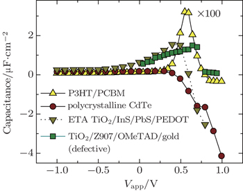
The negative capacitance (NC) in solar cell was first reported in 2006,[1] then there are several reports on NC in different solar cells at high bias voltage.[1518] In these measurements, the solar cell is set in the dark or at fixed illumination. The characteristic behaviors of the terminal capacitance are shown in Fig. 1. Due to the complexity of capacitance, the focus of these papers is merely on the experimental results of NC,[1,1518] or using the simple circuit to model the NC.[18] So far, the mechanism of the NC is still unknown. Generally, the terminal capacitance of solar cell is mainly contributed by the chemical capacitance, which increases with the forward bias. However, in figure 1 the terminal capacitance increases exponentially just at low voltages, then it becomes negative after passing a maximum value. Therefore, aside from the chemical capacitance, there must be another mechanism contributing to the negative values of the terminal capacitance in DSCs.

Fig. 1. Characteristic results of solar cells showing negative capacitance at forward bias:[1,18] a polycrystalline CdTe solar cell, an extremely thin absorber (ETA) cell based on rough TiO2, a dye-sensitized solar cell (defective) with the solid OMeTAD hole conductor, and a normal P3HT/PCBM bulk heterojunction organic solar cell.
3. Analytical analysis of recombination under AC perturbation

Generally, in the semiconductor transport layer of DSCs, the transport of injected free electron concentration, n, satisfies the well-known equation for diffusion, recombination, and generation at steady state[2,19]

where Dn is the electron diffusion coefficient, Un is the recombination rate per unit volume and is often expressed as Un = knβ,[1821] and G is the generation rate, which is so small in electronic transport area and could be ignored in analysis. Hence, under AC perturbation, equation (1) should be reexpressed as[2]

In order to avoid any complication of boundaries, we consider infinite space −∞ < x < ∞ firstly and assume the injection of carriers by a point source at x = 0.[22] Since equation (2) is clearly symmetrical, we only need to consider the half space 0 < x < ∞. The boundary conditions are as follows.[19]

At x = 0, the concentration of injection carriers over the background is determined by the incident photon flux I0; Jin j = qAI0, where q is the electronic charge and A is the ratio of absorbed photon flux to I0.[22]

At x = +∞, n = nb is the equilibrium carrier concentration with no bias voltage and in the dark. The schematic of a dye-sensitized nano-crystalline solar cell is shown in Fig. 2.

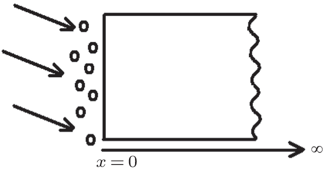
Fig. 2. Schematic of a dye-sensitized nanocrystalline solar cell.

For a DSC, considering the well contact with the substrate and high conductivity of the electrolyte, we can relate the free injected electron density and the voltage VF as[1824]

where kB is Boltzmann’s constant, T is the temperature, q is the elementary charge, and VF is the difference between the electron quasi-Fermi level EFn and the hole quasi-Fermi level FFp, namely, VF = (EFnEFp)/q, and nb is an equilibrium concentration. On the other hand, VF = VappIRs, where Vapp is the applied bias voltage and Rs is the contact resistance of electron or hole poles (see Fig. 3).[18] However, in order to simplify the calculation we will ignore the voltage drop on the contact resistance Rs because the increasing technology and characterization methods could extract accurately it. Therefore, the voltage drop on space 0< x < ∞ is approximately equal to the difference of the quasi-Fermi level.

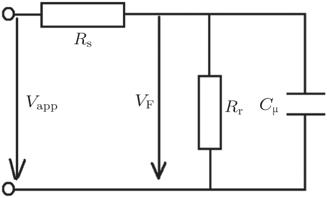
Fig. 3. Equivalent circuit of a dye-sensitized nanocrystalline solar cell.

Suppose that the DC bias voltage dropping on the area 0 < x < ∞ is perturbed by a small signal V2eiωt (we could also choose current as the perturbation, and the analytic method and results are the same), then , where ω is the frequency of the AC small-signal. The total voltage dropping on the area is

The injection carriers’ concentration equation (3) at any point could be expressed as[25]

where n1(x) and n2(x) are caused by DC bias and AC perturbation, respectively. Substituting the carries’ concentration equation (5) into the carriers’ transportation equation (2), and assuming Un = knβ and β = 1,[1820] we have

Time-related and unrelated items can be separated, so equation (6) could be rewired as[25]

The solutions of Eqs. (7) and (8) are

where

LN reflects the relation between the carriers’ exponential decay and their transmission distance, which shows that this parameter corresponds to the average value of the distance traveled by the particles before they disappear by recombination.[2628] The k is the carriers’ recombination rate and equals 1/τ, where τ is the carriers’ lifetime. characterizes the behavior of the carriers caused by small signal perturbation;[19] A1, A2, A3, and A4 are constants and should be determined by the above boundary conditions. Equations (9) and (10) must converge, so items with positive indices x must be discarded, namely, A2 = A4 = 0. Furthermore, from boundary condition (i) one have A1 = n1(0)−nb = Jin j/(qv) = AI0/v, where v is the average drift velocity of electrons. On the other hand, carriers’ concentration should meet Eq. (3). Using Eq. (4) and series-expansion method and ignoring the higher-order infinitesimal, we obtain

Comparing Eq. (13) with Eq. (5), we have

Hence, A1 and A3 can be obtained and the total free electron density is

Using Eq. (15) we obtain the recombination current density as

We can define Jd = qknbLN as the constant parameter, the dark current density, or reverse saturation current density. Equation (16) is abbreviated as

The first item on the right of Eq. (17) has no relation with alternate current; we only consider the last item which can be defined as the AC current density Jrac

The small signal perturbation admittance caused by recombination is

where S is the cross-sectional area, Is = JdS is the dark current or reverse saturation current. From Eq. (17) one can obtain the recombination resistance Rrac and capacitance Crac caused by small signal perturbation and the Rrdc caused by DC bias voltage

In Eq. (22) the sign ‘−’ confirms that the recombination current displays an inductance effect; that is, recombination contributes the negative capacitance to DSCs, and its absolute value has an e-exponential increase with voltage. Generally, capacitance is defined as derivative of accumulated charge with respect to applied voltage, i.e., C = dQ/dVj. When the applied voltage reaches a certain value, the radioactive recombination results in negative variation of total quantity of the injected carriers in the active region, i.e., dQ becomes negative. Then capacitance becomes negative because dVj is positive. On the other hand, the chemical capacitance Cμ for band electrons per across-section is[18]

Comparing Eq. (23) multiplied by S with Eq. (22), we found that although Crac is negative but Cμ is positive, and its absolute value is greater than that of Crac. Therefore, in order to gain the negative terminal capacitance, Crac should series with Cμ. Then the simple equivalent circuit shown in Fig. 2 should be modified as that in Fig. 4. This novel circuit is similar but can explain negative terminal capacitance of DSCs. In it the recombination resistance Rr, we think, should in parallel with recombination capacitance Cr. However, after accurately analyzing the experiments shown in Fig. 1, we found that the capacitance is nearly a constant under reverse bias and small voltage; with increasing voltage, it will pass a maximum value before it becomes NC. Therefore, we believe that there must be a small Helmholtz capacitance between the FTO and the electrolyte of the photo-anode.

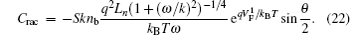
Fig. 4. Equivalent for small AC perturbation, which can explain the NC. Rc is the total series resistance generally caused by constant resistance of the cell; Rr is the recombination resistance including Rrac and Rrdc, and Cr is the recombination capacitance relate the electron transport process in film; Cμ is the chemical capacitance that stands for the change of electron density as a function of the Fermi level; Rct is a charge-transfer resistance related to the traditional recombination of free carriers at electrolyte interface.

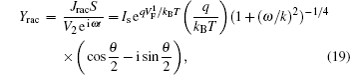
Furthermore, from Eqs. (17) and (18) we find that the recombination resistances Rrac and Rrdc both exponentially decrease with increasing voltage, as shown in Figs. 5(a) and 5(b).

Fig. 5. Calculation results from model of Fig. 1. Behaviors of recombination resistances (a) Rrac and (b) Rrdc caused by AC small signal perturbation and DC, respectively; dependences of (c) Rrac and (d) Crac on frequencies at different values of k (namely 1/τ). We do not consider the product of other factor because these product only change the magnitude of Rrac and Crac without changing the relationship between them and the frequency.

The same relation between the recombination resistance and DC bias voltage has been implied by Eq. (11) in Ref. [21]. Interestingly, Rrdc does not relate with frequency, but Rrac relates; namely, at a fixed value of k, Rrac increases with the frequency as shown in Fig. 5(c). This frequency characteristic of Rrac should relate to the response time of AC signal and carrier lifetime. In Eq. (19), the dependence of NC on voltage is very obvious. Therefore, in Fig. 5(d) we only present the frequency characteristics of NC. It can be seen that at a fixed voltage the lower the frequency is, the more obvious the NC is. This result is fully consistent with the NC phenomenon observed in different devices.[4,814]

4. Summary

A detailed analysis on the recombination behavior of carriers from the carriers’ transport process in DSC confirms that recombination behavior of carriers could contribute to negative capacitance (NC) which had been confirmed experimentally under small-signal perturbation. These expressions also imply that NC relates with frequency, and the lower the frequency is the more obvious the NC is. Furthermore, the recombination resistance should include two parts: one is Rrac caused by AC small-signal perturbation and the other is Rrdc caused by direct-current (DC) bias voltage, and both decrease with the increasing bias voltage. Which one plays a major role relates to the external conditions, such as the frequency of the AC small-signal and the carriers’ lifetime.

Reference
1Iván M SJuan BFrancisco F SGerm‘a GBGuillaume ZKen DYuri PIIona OAbdelhak BThomsa DRamón T ZAbou KClaude L CVincent BStuart J C I 2006 Nano Lett. 6 640
2Zhang L MRobert ECui D L2011J. Phys. Chem. C1161293
3 G HChen HWang X QPang HZhang G LZou BLee H J 2010 Chin. Phys. B 19 085202
4Gommans H H PKemerink MJanssen R A J 2005 Phys. Rev. B 72 235204
5Ali B 2015 Chin. Phys. B 24 047205
6Ma WZhang FMeng S 2014 Chin. Phys. B 23 086801
7Hao J YXu YZhang Y PChen S FQin DLi X AWang L HHuang W 2015 Chin. Phys. B 24 045201
8Martens H C FHuiberts J NBlom P W M 2000 Appl. Phys. Lett. 77 1852
9Hulea I NVan der Scheer R F JBrom H BLangeveld-Voss B M WVan Dijken ABrunner K 2003 Appl. Phys. Lett. 83 1246
10Li NGao X DXie Z TSun Z YDing X MHou X Y 2011 Chin. Phys. B 20 027306
11Gommans H H PKemerink MAnderson G GPijper R M T 2004 Phys. Rev. B 69 155216
12Pingree L S CScott B JRussell M TMarks T JHersam M C 2005 Appl. Phys. Lett. 86 073509
13Feng L FLi YLi DHu X DYang WWang C DXing Q Y 2012 Appl. Phys. Lett. 101 233506
14Ehrenfreund ELungenschmied CDennler GNeugebauer HSariciftci N S 2007 Appl. Phys. Lett. 91 012112
15Germá G BAntoni MEva M BJuan BIrati URoberto P 2008 Org. Electron. 9 847
16Tina C LMárcio S GFrancisco F SJuan BPaulo R BChaiya PJoseph T HTobin J M 2009 J. Phys. Chem. C 113 18385
17Yahia I SMansour S AHafez H SOcakoglu KYakuphanoglu F 2012 J. Inorg. Organomet. P 22 1240
18Juan B 2011 Phys. Chem. Chem. Phys. 13 4679
19Juan BIván M S 2010 J. Phys. Chem. Lett. 1 450
20Juan BFrancisco F SIván M SGermá G BGiménez S 2009 J. Phys. Chem. C 113 17278
21Barea E MZafer CGultekin BAydin BKoyuncu S Icli SFrancisco F SJuan B 2010 J. Phys. Chem. C 114 19840
22Huang S YSchlichthöri GNozik A JGrätzel MFrank A J 1997 J. Phys. Chem. B 101 2576
23Juan B 2010 J. Electroan. Chem. 646 43
24Juan A AJesús IGuillén EJulio V CHumberto J M RGerko OLaila PEmilio P 2012 Phys. Chem. Chem. Phys. 14 10285
25Liu C WZhou X Y W JWang M TQiu Z LMeng W LChen J WQi J JDong C 2015 Acta Phys. Sin. 64 038804 (in Chinese)
26Gonzalez-Vazquez J PJuan A AJuan B 2010 J. Phys. Chem. C 114 8552
27Yang jZhao D GJiang D SLiu Z SChen PLi LWu L LLe L CLi X JHe X GWang HZhu J JZhang S MZhang B SYang H 2013 Chin. Phys. B 22 098801
28Liu J YSong PWang FWang Y 2015 Chin. Phys. B 24 097801