
Image potential states mediated STM imaging of cobalt phthalocyanine on NaCl/Cu(100)
[Guo Qinmin1, Qin Zhihui1, Huang Min1, Mantsevich Vladimir N.2, Cao Gengyu1, †,  ]
]
]
|
|


† Corresponding author. E-mail:
Project supported by the National Natural Science Foundation of China (Grant Nos. 21203239 and 21311120059) and RFBR (Grant No. 13-02-91180).
The adsorption and electronic properties of isolated cobalt phthalocyanine (CoPc) molecule on an ultrathin layer of NaCl have been investigated. High-resolution STM images give a detailed picture of the lowest unoccupied molecular orbital (LUMO) of an isolated CoPc. It is shown that the NaCl ultrathin layer efficiently decouples the interaction of the molecules from the underneath metal substrate, which makes it an ideal substrate for studying the properties of single molecules. Moreover, strong dependence of the appearance of the molecules on the sample bias in the region of relatively high bias (> 3.1 V) is ascribed to the image potential states (IPSs) of NaCl/Cu(100), which may provide us with a possible method to fabricate quantum storage devices.
In the last few decades, many components of molecular circuits, e.g., molecular wires, rectifiers, switches, and transistors, have been fabricated with single molecules.[1–4] The performance of the molecular devices is strongly dependent on the distribution of the molecular orbital. A scanning tunneling microscope (STM) provides with a powerful tool to directly image the molecular orbital in real space. Normally, STM images give us information about both the topography and electronic states of a surface. Since the density of states (electronic structures) of a surface are usually strongly dependent on the energy alignment, the features in STM images are changing with the scanning parameters. Moreover, the electronic states of the adsorbate and substrate would be coupled and contribute to the measured STM images simultaneously. Especially, the electronic states of the STM tips also influence the imaged electronic states greatly. To fully understand the distribution of the molecular orbital, the electronic states involved in STM images have to be clarified.
Electrons in front of metal surfaces would induce image charges and thus feel the attractive force from the image charges. However, they will be reflected by the metal surfaces with high possibility if the metal surfaces, e.g. Cu(100) and Ag(100), have band-gaps involving into the energy of these electrons.[5,6] As a result, electrons above metal surfaces would be trapped by this electrostatic image potential, leading to a pronounced Rydberg-like series of additional surface states existing at these metal surfaces, namely, image-potential states (IPSs). The IPSs can be described as

In this paper, we carry out an STM investigation on a well-known dye molecule, namely, cobalt phthalocyanine (CoPc), on NaCl/Cu(100), where IPSs play a key role.[17] It is found that the molecules on NaCl/Cu(100) appear as dimming holes when the bias voltage exceeds the threshold of 3.1 V. Such an unusual bias-dependent feature of CoPc in STM imaging is ascribed to the IPSs of NaCl/Cu(100). Furthermore, we obtain a highly resolved STM image of the lowest unoccupied molecular orbital (LUMO) of CoPc, which is improved by the adsorption of a single molecule on the tip apex. Understanding the influences of IPSs on orbital imaging would help us improve the performance of molecular devices.
The experiment was carried out in an ultra-high vacuum (UHV) chamber (base pressure 1.3×10⁻⁸ Pa) equipped with a commercial low-temperature STM (Unisoku, Japan). The Cu (100) single crystal surface (Mateck, Germany) was cleaned by cycles of Ar+ sputtering and UHV annealing. The quality of the obtained Cu (100) surface was checked by STM scanning and then the surface was used for deposition. NaCl was thermally evaporated (0.2 ML/min) from a silica evaporator onto Cu (100) kept at room temperature (RT). CoPc molecules, after degassing for more than 20 h, were deposited onto the NaCl/Cu(100). During the deposition, the substrate was kept at 150–200 K in order to reduce the diffusion of molecules as much as possible, and the vacuum was better than 6.6×10⁻⁸ Pa. An electrochemically etched polycrystalline tungsten wire was used as the STM tip. Before measurement, the tip was treated by electron-beam bombardment to get rid of the contamination and oxidation. The bias voltage refers to the sample voltage with respect to the tip, and all topographic images were obtained in constant current mode at ∼ 78 K.
To better understand the adsorption behavior of CoPc on the NaCl/Cu(100) system, we performed plane-wave basis density functional theory (DFT) calculations with Perdew–Burke–Ernzerhof (PBE) generalized gradient corrected approximation (GGA)[20] and ultrasoft pseudopotentials.[21] The cutoff energy for the plane-wave expansion is set to be 400 eV. The Cu(100) surface, cleaving perpendicular to the [100] of the face centered cubic Cu solid, is modeled by a (8×8×3) supercell with 64 Cu atoms per layer. The inter-Cu layer distance is around 1.81 Å. Similarly, the NaCl(100) surface is modeled by a (5×5×4) supercell containing 4 atomic layers with 25 Na atoms and 25 Cl atoms per layer. The inter-NaCl layer distance is around 2.81 Å. The vacuum thickness of 15 Å is set to avoid the interactions between adjacent supercells. The CoPc (C32H16CoN8) molecule is adsorbed on one side of the supercells and the atomic positions are relaxed according to the Hellmann–Feynman forces until the maximum atomic force is less than 0.02 eV/Å. The coordinates of the atoms in the upper part of the slab (containing the CoPc molecule and 2 atomic layers of substrates) are relaxed while the atoms in the lower part of the slab (1 atomic layer for the Cu(100) surface and 2 atomic layers for the NaCl(100) surface) are constrained to their bulk positions. The optimized distances of the CoPc molecule relative to Cu(100) and NaCl(100) are 2.8 Å and 3.2 Å, respectively. The adsorption energy is calculated by: Eads = ECoPc + Esurf − ECoPc/surf, where ECoPc is the total energy of an isolated CoPc molecule, Esurf is the total energy of the clean supercell slab, and ECoPc/surf is the total energy of the supercell slab with one CoPc molecule adsorbed.
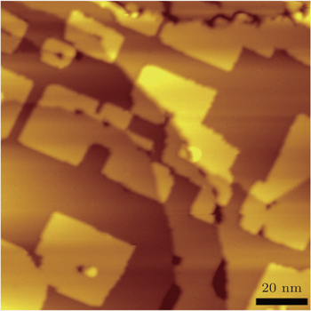
NaCl layers with nominal coverage of 2.2 ML (1 ML refers to a monolayer of NaCl) were grown on Cu(100) at room temperature as shown in Fig.
 | Fig. 1. Large-scale (200 nm×200 nm, Vb = 1.5 V, It = 100 pA) STM image of NaCl film grown on Cu(100) with coverage of 2.2 ML. |
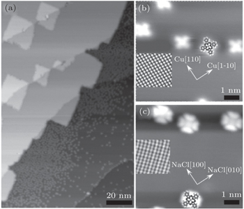
Figure
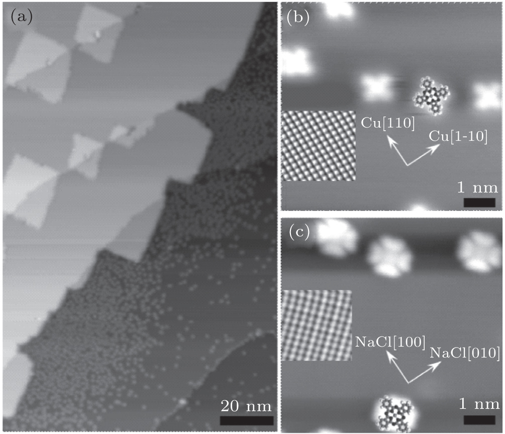 | Fig. 2. (a) CoPc molecules adsorbed on NaCl-partially-covered Cu(100) (100 nm×160 nm, Vb = 3.5 V, It = 65 pA). (b) The molecules on Cu(100) (11 nm×11 nm, Vb = 1.5 V, It = 80 pA) and (c) NaCl layers (11 nm×11 nm, Vb = 2.5 V, It = 35 pA). The insets in panels (b) and (c) are the atomically resolved images of Cu(100) and NaCl/Cu(100), respectively. |
The calculation reveals that CoPc molecules chemisorb on the Cu(100) surface with an adsorption energy of 0.57 eV and physisorb on NaCl with a low adsorption energy of around 0.15 eV. The results indicate that the molecules interact with Cu(100) more strongly. Therefore, the CoPc molecules could diffuse on the NaCl layer readily and be captured by the Cu(100) surface at the preparation temperature (150–200 K). That is why the density of CoPc molecules on Cu(100) near NaCl layers is much larger than that far from NaCl layers.
Although the molecular adsorption is very weak, there are still some molecules located on NaCl layers. Figures
Due to its insulator property, NaCl could efficiently decouple the interaction from the free electrons of the underlying metal substrate.[17–19,25–32] NaCl has no energy bands and surface states near the Fermi level, so NaCl layers just act as tunneling barriers at relatively low sample biases (typically below 3.1 V in the case of the NaCl/Cu(100) system). The adsorbed molecules participate tunneling by their frontier orbitals near the Fermi level, and information about the orbitals of the free molecules can be better extracted like the case of pentacene on NaCl/Cu(111).[18] Since the adsorption energy of CoPc on NaCl is only 0.15 eV, it is feasible to gather a single CoPc molecule onto the tip apex just by fast scanning on the surface of CoPc on NaCl layers. Figure
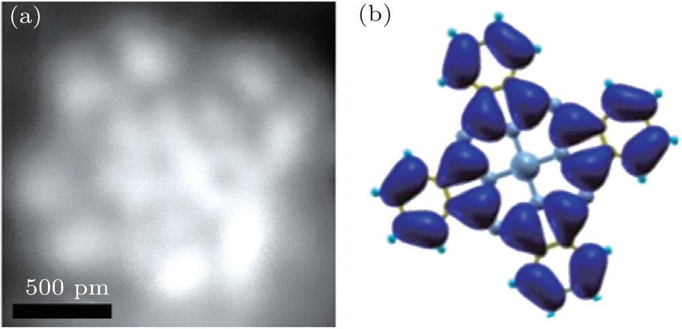 | Fig. 3. (a) STM image of CoPc molecules on NaCl/Cu(100) in sub-molecular resolution (1.8 nm×1.8 nm, Vb = 1.5 V, It = 74 pA). (b) Calculated real-space distribution of LUMO of a free CoPc molecule. |
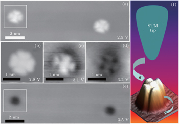
If the tunneling bias exceeds a critical voltage (3.1 V), the tunneling current would suffer a remarkable increase as indicated by the z–V curve in our previous report.[17] We ascribe the increase of the tunneling current to image potential states (IPSs). Indeed, the IPSs originate from the substrate Cu(100), and could be largely blue-shifted by the ad-layer, for example, NaCl layers.[17] Due to the adsorption of the NaCl layers, the first order of IPSs of Cu(100), which is the closest one to the Fermi level (EF), is shifted from ∼ 4.5 eV to ∼ 3.1 eV. In order to further investigate how the IPSs influence the adsorbed CoPc molecules, at least one of the IPSs has to be involved in the tunneling process. For simplicity, the first order of IPSs located energetically at ∼ 3.1 V[17] is chosen here. Unfortunately, we have not acquired STS on CoPc molecules. However, we acquired a series of STM images with different voltages as shown in Figs.
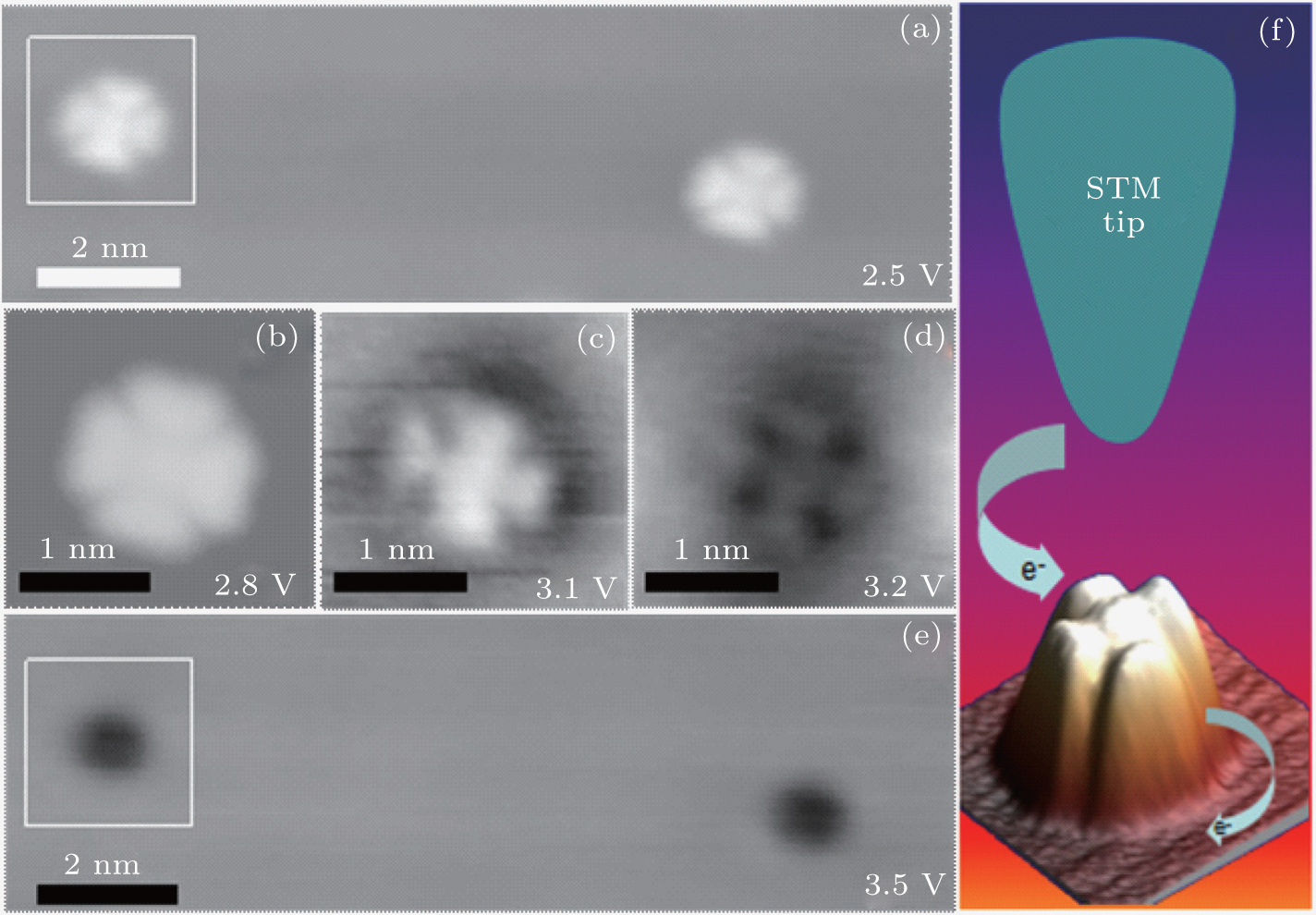 | Fig. 4. A series of STM images obtained at various bias voltages: (a) 2.5 V, (b) 2.8 V, (c) 3.1 V, (d) 3.2 V, and (e) 3.5 V. The STM images in panels (b)–(d) show the CoPc molecule indicated by squares in panels (a) and (e). (f) Two steps of the electron tunneling process in the molecule-covering NaCl region at positive bias voltages. Electrons firstly tunnel from the tip to the empty molecular orbitals and then transfer to the IPSs of the underlying NaCl/Cu(100). The scan sizes of panels (a) and (e) are 4.2 nm×13.0 nm, and the sizes of panels (b)–(d) are 2.5 nm×2.5 nm. The tunneling currents are 16 pA in panels (a)–(e). |
As shown in Fig.
We have investigated the structural and intrinsic electronic properties of individual CoPc molecules adsorbed on the NaCl bilayer supported by Cu(100). Our high-resolution STM image demonstrates that the CoPc molecules adsorb on the NaCl bilayer with their lobes along the NaCl 〈011〉 direction. Due to the decoupling effect of the NaCl layers, the quasi-free CoPc molecular orbital information could be extracted and the best resolution of molecules is achieved using a single molecular tip. Moreover, at bias voltages higher than the first order IPSs of NaCl/Cu(100), the electron tunneling from CoPc into Cu(100) is dominated by the IPSs, resulting in the bias-dependent dimming process of the CoPc molecules. The adsorption of molecules drastically reduces the local density of states of IPSs, which is indicative of the feasibility of fabricating a quantum storage device based on tuning of IPSs by molecular adsorption.
| 1 | |
| 2 | |
| 3 | |
| 4 | |
| 5 | |
| 6 | |
| 7 | |
| 8 | |
| 9 | |
| 10 | |
| 11 | |
| 12 | |
| 13 | |
| 14 | |
| 15 | |
| 16 | |
| 17 | |
| 18 | |
| 19 | |
| 20 | |
| 21 | |
| 22 | |
| 23 | |
| 24 | |
| 25 | |
| 26 | |
| 27 | |
| 28 | |
| 29 | |
| 30 | |
| 31 | |
| 32 |