Image potential states mediated STM imaging of cobalt phthalocyanine on NaCl/Cu(100)
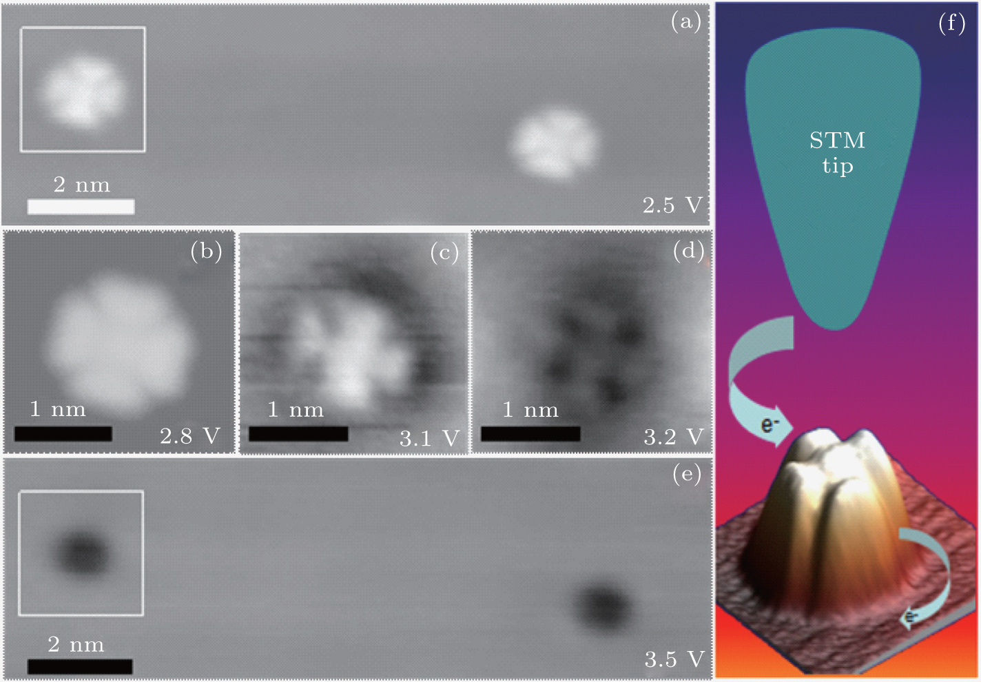
A series of STM images obtained at various bias voltages: (a) 2.5 V, (b) 2.8 V, (c) 3.1 V, (d) 3.2 V, and (e) 3.5 V. The STM images in panels (b)–(d) show the CoPc molecule indicated by squares in panels (a) and (e). (f) Two steps of the electron tunneling process in the molecule-covering NaCl region at positive bias voltages. Electrons firstly tunnel from the tip to the empty molecular orbitals and then transfer to the IPSs of the underlying NaCl/Cu(100). The scan sizes of panels (a) and (e) are 4.2 nm×13.0 nm, and the sizes of panels (b)–(d) are 2.5 nm×2.5 nm. The tunneling currents are 16 pA in panels (a)–(e).

