

Investigations of the optical properties of Si surface with microwires for solar cell applications
[Li Li1, Wu Shi-Liang1, Yu Dong1, Wang Wei1, Liu Wen-Chao2, Wu Xiao-Shan1, Zhang Feng-Ming1, †,  ]
]
]
|
|


† Corresponding author. E-mail:
Project supported by the National Natural Science Foundation of China (Grant Nos. U1332205, 11274153, 11204124, and 11404091).
Combined with the rough textures which are usually used for fabricating the planar solar cells, textured-microwire (MW) structures (there are MW textures on the tops of MWs) are fabricated. Both simulative and experimental investigations of the optical properties of Si surface with microwires are carried out and the results show that surfaces of textured-MW structures exhibit lower reflectance in the short wavelength range, but higher reflectance in the long wavelength range than the conventional textured surface. It is also shown, consequently, that the textured-MW structures could absorb more photons in the short wavelength range, which could help improve the performance of the solar cells.
In order to achieve higher efficiency, many approaches have been proposed. Using a low-reflection surface is one of the most effective ways.[1–8] Yablonovitch[9] used a statistical approach to study the optical properties of the media with complicated surfaces like random textured surfaces, while Campbell and Green[10] studied the light trapping properties of pyramidal textured surfaces. These two kinds of surface structures have been widely used in today’s industry to reduce the reflection of silicon solar cells. Recently, solar cells with nano-structured surfaces have attracted a lot of attention, like black silicon[11–13] which exhibits an outstanding antireflection ability. Besides quite a low reflection, nanowire solar cells[14–18] with radial pn junctions can relax the requirement for the quality of materials by decoupling the direction of incident light absorption and the direction of photon-generated carriers’ collection. So high-efficiency solar cells can be fabricated with low-quality materials by using this special radial junction structure.
However, little improvement of performance has been observed in experiments on these nano-structured solar cells,[19] and one of the main reasons is the poor quality of radial pn junctions.[16] So some groups studied solar cells with columnar arrays on the order of micrometers.[20–23] This kind of structure can also achieve the purpose of relaxing the requirement for material quality. As the conventional tube-furnace diffusion method is applicable to the microwires (MWs) and no dead layer problem occurs, it would be easy to fabricate MW solar cells with high-quality radial junctions in a low-cost way compared with fabricating the nanowire solar cells.
It is worthwhile to study the optical properties of these solar cells with radial junctions in order to improve their performances. Many groups have reported the results about low reflectivities of nanowires both experimentally and simulatively, which are mainly contributed by their special surface structures on a sub-wavelength scale.[24,25] Unlike nanowires, wires of micron-scale radius are expected to exhibit different optical properties on their different scales. Kosten et al.[26] developed a ray optics model to investigate the light trapping observed in silicon MWs. The calculated results showed that with the Lambertian back reflector, MWs could exceed the ergodic limit in the ray optics regime. Lee et al.[27] compared the experimental and simulative reflectance results of Si MW solar cells, showing that the reflectance of MWs all exceeded 30% in the range of visible light, which is much higher than that of nanowire solar cells. So it is important to reduce the reflectivities of MWs in order to improve the performance of cells. Based on the fact that wet-chemically textured surfaces are widely used in the photovoltaic industry, presented here is an investigation on the scenario of combining the structure of MWs and the textured surfaces for improving the optical properties of cells. As have been observed in nano-scale structures,[28,29] changing the radii of MWs would affect the optical properties of structures.
Multi-crystalline silicon solar cells with conventional textured surfaces and textured-MW structured (with textures on the tops of MWs) surfaces with different radii have been fabricated. By comparing with the conventional textured surface prepared by acid etching, textured-MW structured surfaces were prepared with acid etching followed by inductive coupled plasma etching. A PECVD coating procedure was used to prepare the outmost SiNx layer to reduce the reflectivity of the structure. Figure
 | Fig. 1. Cross section image of textured-MWs. |
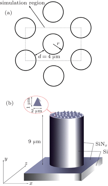
 | Fig. 2. Unit cell of simulation, and (b) schematic plot of the calculated textured-MW structure. |
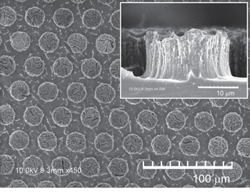
The SEM image of a textured-MW structure sample (r = 12 μm) is shown in Fig.
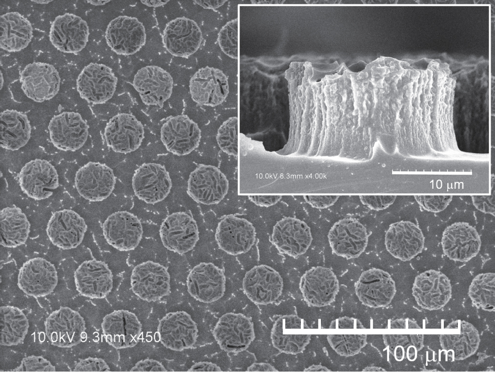 | Fig. 3. The SEM image of a silicon surface with textured-MWs each with a radius of 12 μm. |
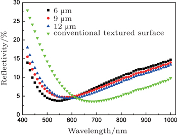
Shown in Fig.
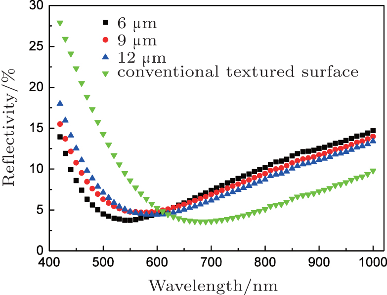 | Fig. 4. Measured reflectivity results of conventional textured surface and textured-MW structured surfaces with different radii (6 μm, 9 μm, and 12 μm). |
Based on the reflectivity (R), wafer thickness (t) and absorption coefficient (α), the absorbed photons n(λ) at wavelength λ can be expressed as

From Eq. (
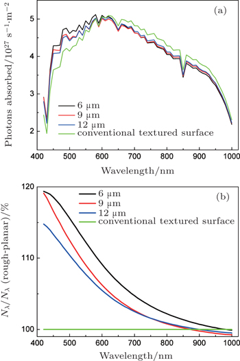
 | Fig. 5. (a) Dependences of the absorbed photons on wavelength, and (b) wavelength dependence of the total photons from 420 nm to 1000 nm, for different radii of textured-MW structured surfaces of 180-μm-thick Si wafers. |
To better understand the effects of MW structures on the performance of solar cells, it is interesting to further analyze the photon absorption in the short wavelength range. The total photons absorbed in a wavelength range from λ0 to λ can be expressed as

By taking the N(λ) of the conventional textured surface as the reference, the increase of N(λ) for the textured-MW structured surfaces in percentage can be obtained from Fig.
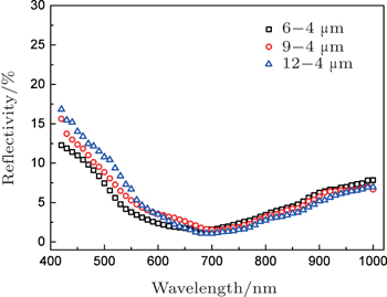
The simulated reflectance results of textured-MW structured surfaces with different wire radii (6 μm, 9 μm, and 12 μm) are obtained with FDTD Solutions and shown in Fig.
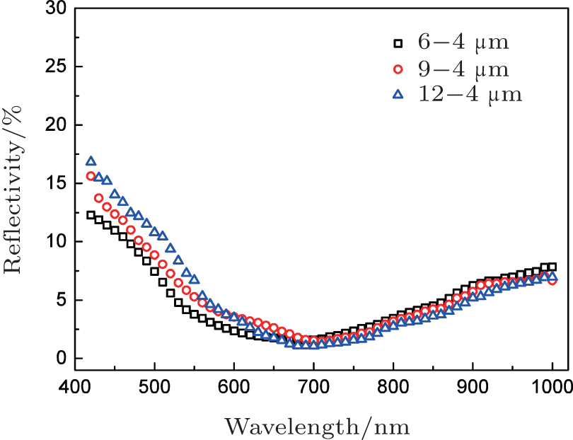 | Fig. 6. Simulated reflectivity results of conventional texture surface and textured-MW structured surfaces with wires of different radii (6 μm, 9 μm, and 12 μm). |
In order to understand the difference in light distribution in Si wafers between conventional textured surface and textured-MW structured surface, their electric field magnitude distributions are calculated. Shown in Fig.
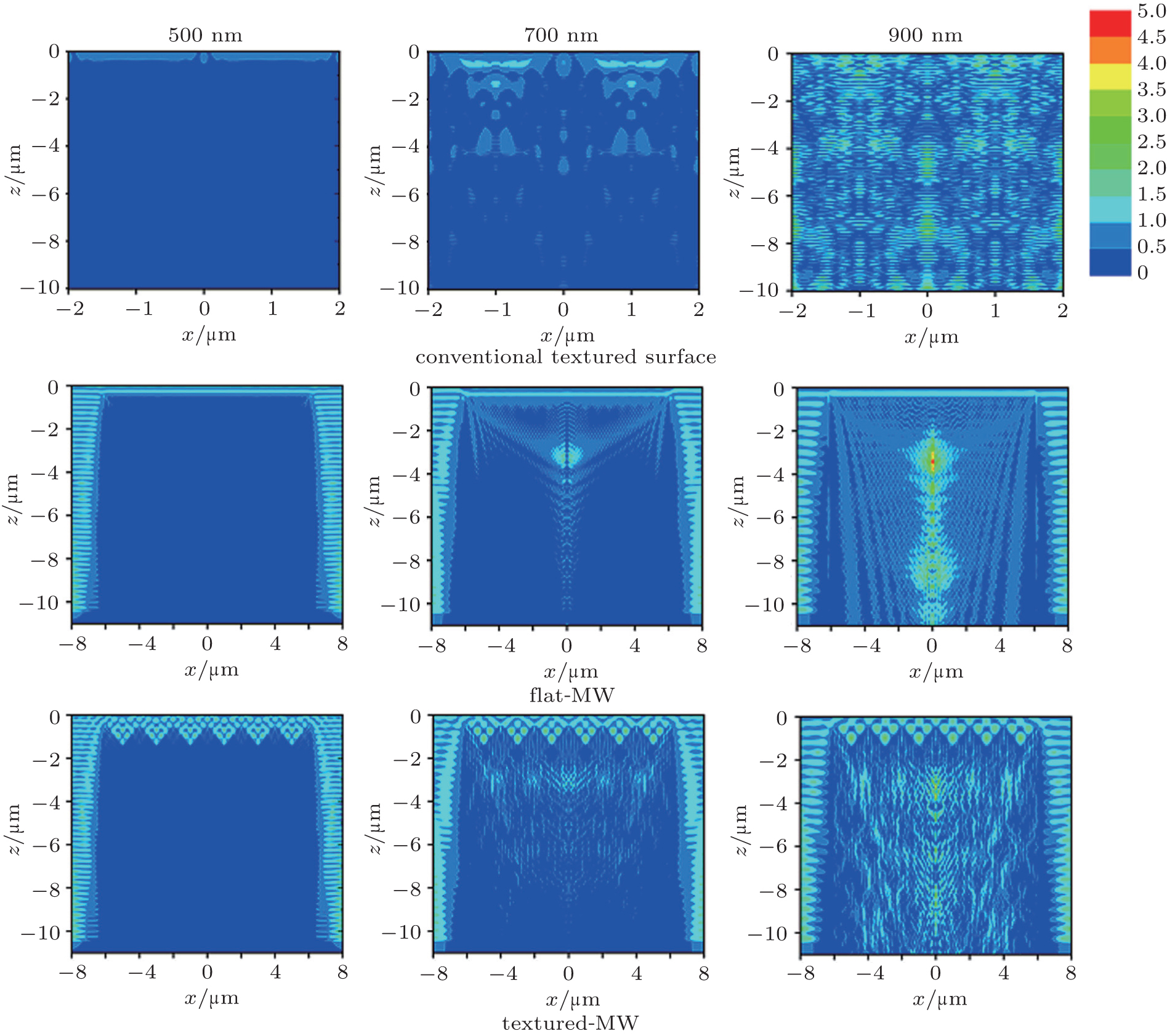 | Fig. 7. Electric field magnitude distributions of three structures (conventional texture surface, flat-MW, and textured-MW) at wavelengths of 500 nm, 700 nm, and 900 nm. |
The reflectivities of conventional textured surface and textured-MW structured surfaces are investigated. The experimental and simulated results are in good agreement with each other. Compared with the conventional textured surface, textured-MWs structures show a lower reflectivity in the short wavelength range and higher reflectivity in the long wavelength range. The surfaces of MWs with smaller radii exhibit lower reflectivities in the short wavelength range, but higher reflectivities in the long wavelength range. Further analysis indicates that textured-MWs can absorb more photons in the short wavelength range, which could help to improve the collection efficiency of carriers. Moreover, simulations on electric field magnitude distributions in the MWs show that textured-MWs structures demonstrate a better effect on the improvement of the carrier collections.
| 1 | |
| 2 | |
| 3 | |
| 4 | |
| 5 | |
| 6 | |
| 7 | |
| 8 | |
| 9 | |
| 10 | |
| 11 | |
| 12 | |
| 13 | |
| 14 | |
| 15 | |
| 16 | |
| 17 | |
| 18 | |
| 19 | |
| 20 | |
| 21 | |
| 22 | |
| 23 | |
| 24 | |
| 25 | |
| 26 | |
| 27 | |
| 28 | |
| 29 | |
| 30 |