Zhang Cheng, Zhou Tong, Liang Sihang, Cao Junzhi, Yuan Xiang, Liu Yanwen, Shen Yao, Wang Qisi, Zhao Jun, Yang Zhongqin, Xiu Faxian. Unexpected low thermal conductivity and large power factor in Dirac semimetal Cd 3 As 2 . Chinese Physics B , 2016, 25(1): 017202
Permissions
Unexpected low thermal conductivity and large power factor in Dirac semimetal Cd 3 As 2
Zhang Cheng 1, 2 , Zhou Tong 1, 2, 3 , Liang Sihang 1, 2 , Cao Junzhi 1, 2 , Yuan Xiang 1, 2 , Liu Yanwen 1, 2 , Shen Yao 1, 2 , Wang Qisi 1, 2 , Zhao Jun 1, 2 , Yang Zhongqin 1, 2, 3 , Xiu Faxian 1, 2, †,
State Key Laboratory of Surface Physics and Department of Physics, Fudan University, Shanghai 200433, China
Collaborative Innovation Center of Advanced Microstructures, Fudan University, Shanghai 200433, China
Key Laboratory for Computational Physical Sciences (MOE), Fudan University, Shanghai 200433, China
Thermoelectrics has long been considered as a promising way of power generation for the next decades. So far, extensive efforts have been devoted to the search of ideal thermoelectric materials, which require both high electrical conductivity and low thermal conductivity. Recently, the emerging Dirac semimetal Cd 3 As 2 , a three-dimensional analogue of graphene, has been reported to host ultra-high mobility and good electrical conductivity as metals. Here, we report the observation of unexpected low thermal conductivity in Cd 3 As 2 , one order of magnitude lower than the conventional metals or semimetals with a similar electrical conductivity, despite the semimetal band structure and high electron mobility. The power factor also reaches a large value of 1.58 mW·m −1 ·K −2 at room temperature and remains non-saturated up to 400 K. Corroborating with the first-principles calculations, we find that the thermoelectric performance can be well-modulated by the carrier concentration in a wide range. This work demonstrates the Dirac semimetal Cd 3 As 2 as a potential candidate of thermoelectric materials.
As a clean, quiet and reliable way of power generation and refrigeration, thermoelectric (TE) phenomena are expected to play an important role in the global sustainable energy solution. [ 1 – 3 ] However, substantial challenge remains unresolved before the wide spread of thermoelectricity due to the low efficiency in heat-to-electricity conversion. [ 1 , 4 ] The TE energy conversion efficiency is evaluated by a dimensionless thermoelectric figure of merit ZT = S 2 σT / κ , where S , σ , T , and κ are the Seebeck coefficient, electrical conductivity, temperature, and thermal conductivity, respectively. One of the most fascinating approaches to design a high-performance TE material is to independently control the thermal and electrical transport. [ 1 , 2 , 5 ] Over the past several decades, extensive efforts have been devoted to this approach involving the study of low-dimensional TE materials and the exploration of phonon glass–electron crystals, aiming at lowering the thermal conductivity while maintaining the high electrical conductivity. [ 1 , 2 , 5 , 6 ]
To maximize ZT, a large Seebeck coefficient, a high electrical conductivity, and a low thermal conductivity are required. These parameters are in fact intimately coupled, providing conflicts in the optimization process. [ 2 ] For example, a high mobility leads to a high conductivity σ ; but usually it is accompanied with a high thermal conductivity κ . On the other hand, the low thermal dissipation and high electrical conductivity in large-mobility materials strike as appealing features during the energy conversion. [ 7 ] A straightforward method to overcome such a trade-off is to reduce the lattice thermal conductivity κ L by introducing the lattice disorder thus shortening the phonon mean free path. [ 7 , 8 ] But it requires the materials to preserve high mobility in the presence of lattice disorder, which is not the case for the most materials available so far. [ 8 ]
Recently, a new class of topological matter, Dirac semimetal, is theoretically predicted and experimentally realized in Cd 3 As 2 . [ 9 – 13 ] In such materials, the conduction band and the valence band intersect each other only at Dirac nodes in the momentum space, forming a semimetal band structure. [ 10 , 13 ] Similar to other Dirac materials like topological insulators, Cd 3 As 2 possesses a linear band dispersion and topological nontrivial band structure. [ 10 , 13 ] Remarkably, transport experiments revealed a hidden protection mechanism that strongly suppressed the backscattering of electrons in the absence of magnetic field, leading to an exceptionally long electron mean free path up to hundreds of micron meters at low temperatures thus holding a great prospect for the high TE performance. [ 14 , 15 ]
In this work, we report the TE properties of this newly-discovered Dirac semimetal Cd 3 As 2 . Remarkably, despite its high mobility, the thermal conductivity of Cd 3 As 2 is found to be unexpectedly low, down to 4.17 W·m −1 ·K −1 , resulting from a large phonon–phonon scattering. [ 16 ] For conventional metals or semimetals with similar electrical conductivity, the thermal conductivity is usually an order larger. [ 17 ] Benefiting from the semimetal band structure, a relatively large Seebeck coefficient is achieved which exhibits a linear dependence on temperature, similar to that of graphene. Owing to the exceptional electrical conductivity, the eventual power factor (PF) in Cd 3 As 2 reaches an extraordinary high value of S 2 σ = 1.58 mW·m −1 ·K −2 at room temperature, several times higher than recently reported TE materials SnSe. [ 18 ] and β -Cu 2 Se. [ 19 ] Meanwhile, its TE properties can be effectively modulated by carrier doping as observed in the Cr-doped samples. A large enhancement of ZT is expected in Cd 3 As 2 with certain doping levels according to our first-principles calculations. Our work clearly establishes Cd 3 As 2 as a brand new candidate of TE materials and provides inspirations on the future investigations of the TE performance in Dirac semimetals.
2. Material growth and charactization
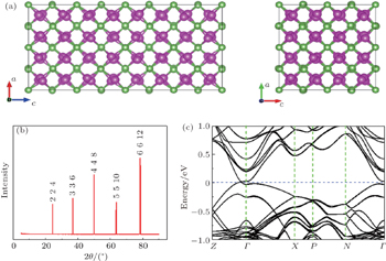
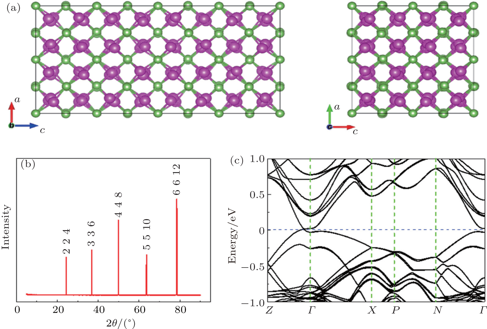
The Cd 3 As 2 single crystals were grown by a self-flux method as elaborated in our previous work. [ 15 ] Stoichiometric amounts of high-purity Cd powder (4N) and As powder (5N) elements were placed inside the alumina crucible with the molar ratio fixed at n (Cd): n (As) = 8:3. The alumina crucible was sealed in an iron crucible under argon atmosphere before being heated to 800 °C and kept for 24 h. After that, the crucible was slowly cooled down to 450 °C at 6 °C per hour and kept at 450 °C for more than one day then cooled naturally to room temperature. The superfluous Cd flux was removed by centrifuging in a vacuum quartz tube at 450 °C. The crystal domain grown by this method was usually below 5 mm. For thermal transport, multi-domain samples were used. The crystal structures of the synthesized crystals were characterized by XRD with Cu K α radiation ( λ = 1.5418 Å). Figures 1(a) and 1(b) show the crystal structure and x-ray diffraction (XRD) pattern of a Cd 3 As 2 single crystal, respectively. It is a distorted superstructure of the antifluorite ( M 2 X ) structure type with an I 4 1/acd space group. It can be viewed as a tetragonally-distorted anti-fluorite structure containing 80 atoms per unit cell and 1/4 Cd site of ordered vacancies. In corroborating with the experimental efforts, we have performed the first-principles band-structure calculations on Cd 3 As 2 with spin–orbit coupling included as shown in Fig. 1(c) . Clearly, a semimetal feature is developed as the conduction band and valance band contact each other at certain points in the momentum space.
Fig. 1. Crystal structure and band structure of Cd 3 As 2 . (a) Crystal structure of Cd 3 As 2 with a distorted superstructure of the antifluorite ( M 2 X ) structure type with an I 4 1/acd space group. The red and green balls represent Cd and As atoms, respectively. (b) XRD of the single crystal Cd 3 As 2 with a (112) crystal surface. (c) The calculated band structures for Cd 3 As 2 , showing a semimetal structure.
3. Thermal and electrical transport result of Cd 3 As 2
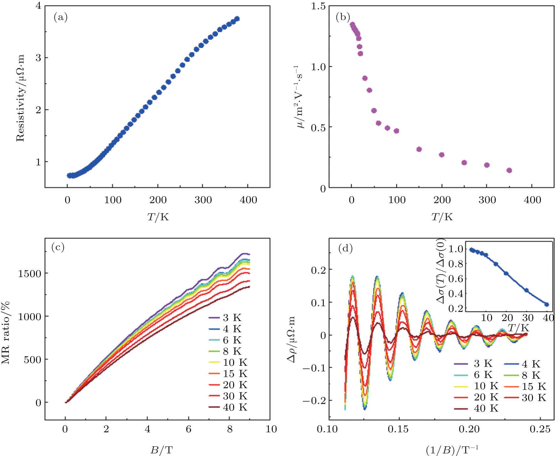
Thermal transport and magnetotransport measurements were conducted in a physical properties measurement system (PPMS) with a thermal transport option and low frequency (< 200 Hz) AC lock-in technique. Magnetoresistivity and Hall coefficients were simultaneously measured down to 2.5 K with a magnetic field applied perpendicularly to the crystal surface. Figure 2(a) is the temperature dependence of electrical resistivity in a typical Cd 3 As 2 single crystal, showing a metallic behavior with saturation at low temperatures, consistent with the calculated band structure. By performing the Hall effect measurements, we found a high electron mobility up to 0.18 m 2 ·V −1 ·s −1 at room temperature, in agreement with previous reports. [ 14 , 15 ] Figure 2(b) is the temperature dependence of mobility that increases to 1.34 m 2 ·V −1 ·s −1 at 3 K. The carrier density is on the order of 10 19 cm −3 . Such a high mobility in Cd 3 As 2 is resulted from the linear band dispersion and the suppression of the electron backscattering. [ 14 ] We also carried out the magnetotransport measurements. Consistent with previous reports, [ 14 , 15 ] linear magnetoresistivity (MR) is observed with a large MR ratio over 1700% at 3 K (Fig. 2(c) ). Strong Shubinikov–de Haas (SdH) oscillations are clearly resolved below 40 K owing to the Dirac band structure and the resultant high mobility. To quantitatively analyze the SdH oscillations, we extract the resistivity oscillation amplitude at different temperatures, which shows a periodic behavior with 1/ B due to the formation of Landau levels under magnetic field (Fig. 2(d) ). The temperature-dependent amplitude Δ σ xx is described by Δ σ xx ( T )/Δ σ xx (0) = λ ( T )/sinh( λ ( T )) with a thermal factor λ ( T ) = 2 π 2 k B Tm cyc /( ħeB ). [ 15 ] where k B is the Boltzmann’s constant, ħ is the reduced plank constant, and is the cyclotron mass. By fitting the normalized conductivity oscillation amplitude (at B = 7.96 T) versus temperature to the equation, we can estimate the carrier effective mass to be m cyc = 0.049 m e .
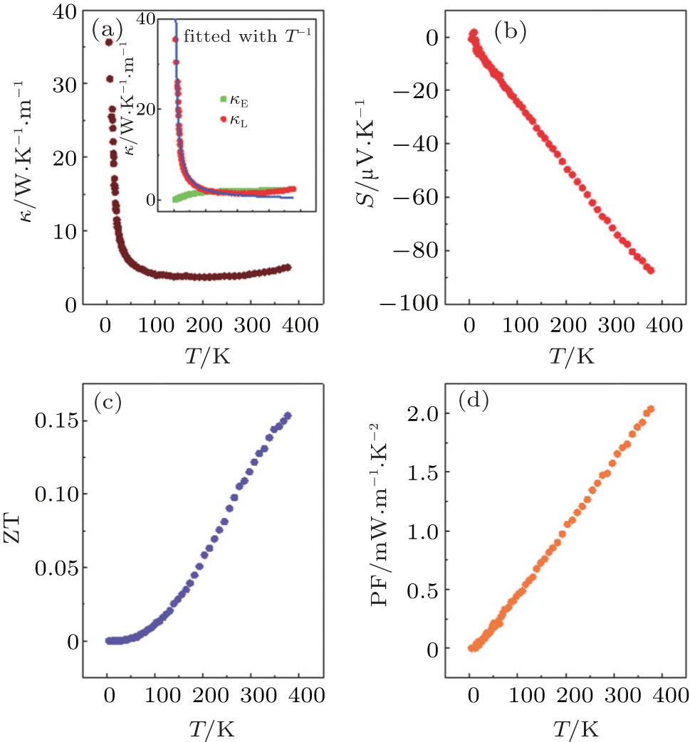
Conventionally, materials with a semimetal band structure and an extremely small carrier effective mass are believed to be a bad choice for thermoelectrics. [ 2 ] However, as we performed the thermal transport measurements on Cd 3 As 2 , the thermal conductivity κ showed unexpected behavior, in spite of the semimetal band structure and electrical transport results. The κ in Cd 3 As 2 is found to be unusually low, comparable to the common amorphous materials, in sharply contrast to its high electrical conductivity. As shown in Fig. 3(a) , κ declines with temperature before showing a significant increase below 50 K. It is well known that the thermal conductivity can be originated from the electron κ E and the lattice κ L contributions. [ 20 ] Here, the electron thermal conductivity κ E can be extracted from the electrical conductivity by using the Wiedemann–Franz law (Fig. 3(a) inset). We notice that the obtained lattice thermal conductivity ( κ L = κ − κ E ) is as low as 1.91 W·m −1 ·K −1 at 300 K. In the temperature range of 200–300 K, κ L slightly decreases as the temperature is reduced. A previous study revealed that the phonon mean free path is extremely short in Cd 3 As 2 , about one interatomic distance, [ 16 ] in stark contrast to the long electron mean free path. [ 14 ] They argued that the phonon scattering from the localized electron transition between As sites was the possible reason of the anomalous low thermal conductivity. [ 16 ] However, in our temperature-dependent thermal transport measurements, a significant enhancement in κ L below 50 K is observed, following a clear T −1 dependence. This behavior strongly supports the fact that the phonon–phonon scattering is the main reason of the low thermal conductivity. [ 21 ] instead of the phonon–electron scattering proposed in the previous study. [ 16 ] At low temperatures, with the increase of phonon mean free path, κ L becomes the major contribution to the total thermal conductivity (also refer to Fig. 3(a) inset). Conventionally, the lattice thermal conductivity increases as the temperature decreases but exhibits an Umklapp peak before following a T 3 relation due to the boundary scattering. [ 8 ] In Cd 3 As 2 , the decrease of κ L from the boundary scattering was not observed down to 4 K owing to the large crystalline size, consistent with a recent report. [ 22 ] Same as the Hall effect, the Seebeck coefficient S shows a negative sign, indicating the electron-type conduction (Fig. 3(b) ). At room temperature, the value of S reaches −74.1 μV·K −1 , which is comparable to previously-studied semi-metallic TE material β -CuAgSe. [ 7 ] The temperature dependence of S adopts a linear relationship over a wide temperature range (2–380 K), reminiscent of that in graphene. [ 23 ]
Fig. 2. Electrical transport properties of Cd 3 As 2 . (a) and (b) Temperature-dependent resistivity and mobility of Cd 3 As 2 , respectively. (c) The MR ratio as a function of B , with distinct SdH oscillation observed at low temperatures. (d) Extracted resistivity oscillation amplitude at different temperatures. The inset in panel (d) is the normalized conductivity amplitude versus temperature which can be used to estimate the carrier effective mass by fitting to the equation Δ σ xx ( T )/Δ σ xx (0) = λ ( T )/sinh( λ ( T )).
Currently, most of the TE materials such as SiGe and skutterudites show a large ZT value at high temperature regime (over 600 K). [ 2 , 24 ] Only a few materials including Bi 2 Te 3 and Sb 2 Te 3 have a large ZT around 1 at room temperature in the bulk form. [ 2 ] Thus, more TE material candidates with high room-temperature ZT are needed for the practical applications. Here, the high mobility and low thermal conductivity in Cd 3 As 2 persist from 50 K up to 380 K. For a better assessment of the TE properties, we calculated the temperature dependence of ZT and PF as shown in Figs. 3(c) and 3(d) , respectively. Both of them increase monotonically with temperature in the range of 2–380 K. The ZT reaches 0.15 at 380 K. Although the ZT value needs further improvement, PF in Cd 3 As 2 reaches an unexpected large value of 2.03 mW·m −1 ·K −2 at 380 K, similar with the BiSbTe bulk alloy [ 25 ] and the recently-reported SnSe single crystal. [ 18 ] In general, the high PF requires both a large Seebeck coefficient and a high electrical conductivity. For a system with a fixed carrier concentration, PF is expected to scale with the effective mass m * and mobility μ . [ 2 ] Here, the exceptional large electron mobility compensates the small effective mass from the linear band dispersion, leading to the obtained high PF in Cd 3 As 2 .
Fig. 3. Thermal transport properties of the undoped Cd 3 As 2 . (a)–(d) Temperature-dependent thermal conductivity, Seebeck coefficient, ZT and PF of the undoped Cd 3 As 2 , respectively. The inset in panel (a) is the extracted electron and lattice thermal conductivity based on the Wiedemann–Franz law.
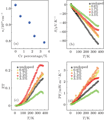
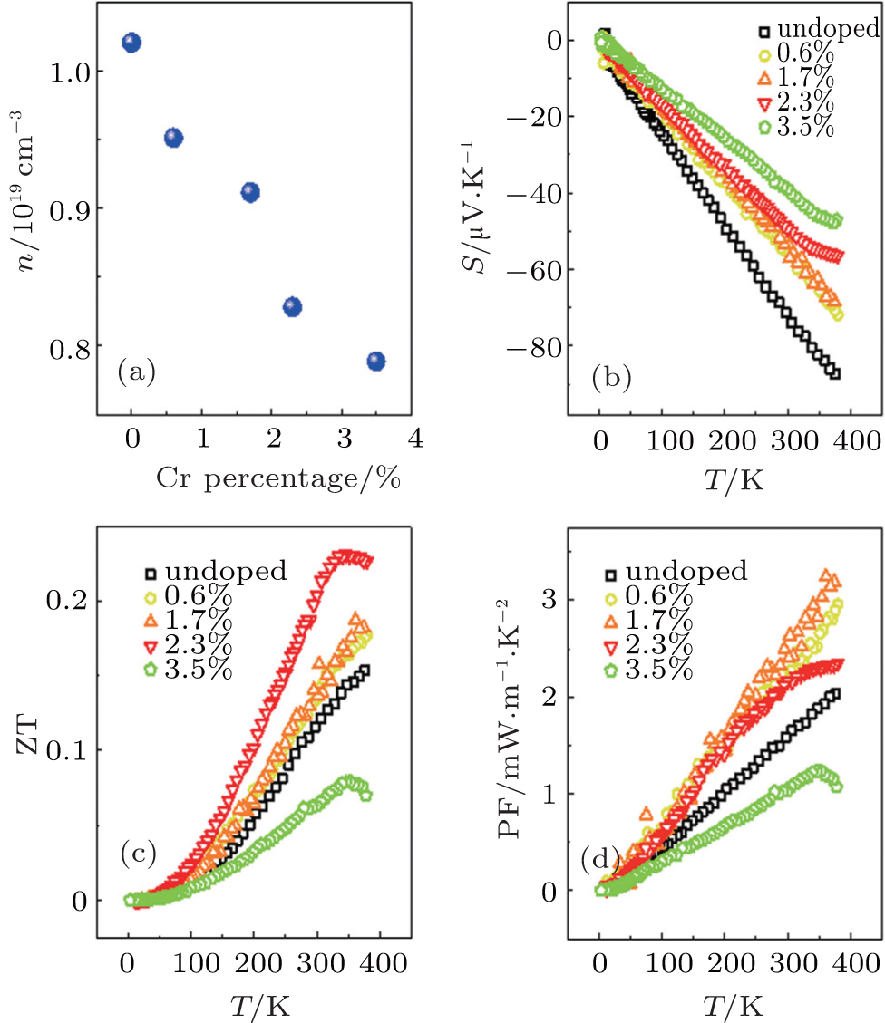
Carrier concentration is also a crucial parameter for TE materials, which is closely related to the Seebeck coefficient S and electrical conductivity σ . To verify the doping effect on the thermoelectric performance in Cd 3 As 2 , we produced Cr-doped Cd 3 As 2 with different doping concentrations and performed the thermal transport measurements. Cr doping is achieved by adding different amount of Cr power into the source. The doping concentrations were determined by energy dispersive spectroscopy through scanning electron microscope. No long-rang ferromagnetic order is induced by the Cr dopant. As shown in Fig. 4(a) , the carrier density in doped Cd 3 As 2 decreases with the increase of Cr doping concentrations (in atomic ratio). Correspondingly, S decreases as n declines (Fig. 4(b) ). Usually, the introduction of external dopants can affect S in two ways: the carrier density n and Fermi level E F , thus modifying the density of states near E F . However, in Dirac materials, the linear dispersion leads to a negligible influence on the density of states within a small range of Fermi energy. Thus, the doping effect on the TE properties of the samples is primarily through the change of the carrier density. Figures 4(c) and 4(d) reveal the ZT and PF in the doped samples as a function of temperature. Although S is reduced upon Cr doping, the value of ZT can be further optimized to 0.22 with 2.3% Cr doping. Further increasing the Cr doping level leads to the significant reduction of the ZT and PF that is mainly due to the decrease of the mobility and electrical conductivity. Hence, another suitable doping element is required to tune the system to optimized condition.
Fig. 4. Electrical and thermal transport properties of Cr-doped Cd 3 As 2 . (a) Changes of carrier density with different Cr doping concentrations (atomic ratio) at 300 K. (b)–(d) Temperature-dependent Seebeck coefficient, ZT and PF of Cr-doped Cd 3 As 2 , respectively.
4. Theoretical study of the TE properties of Cd 3 As 2
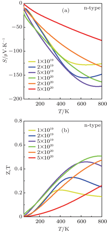
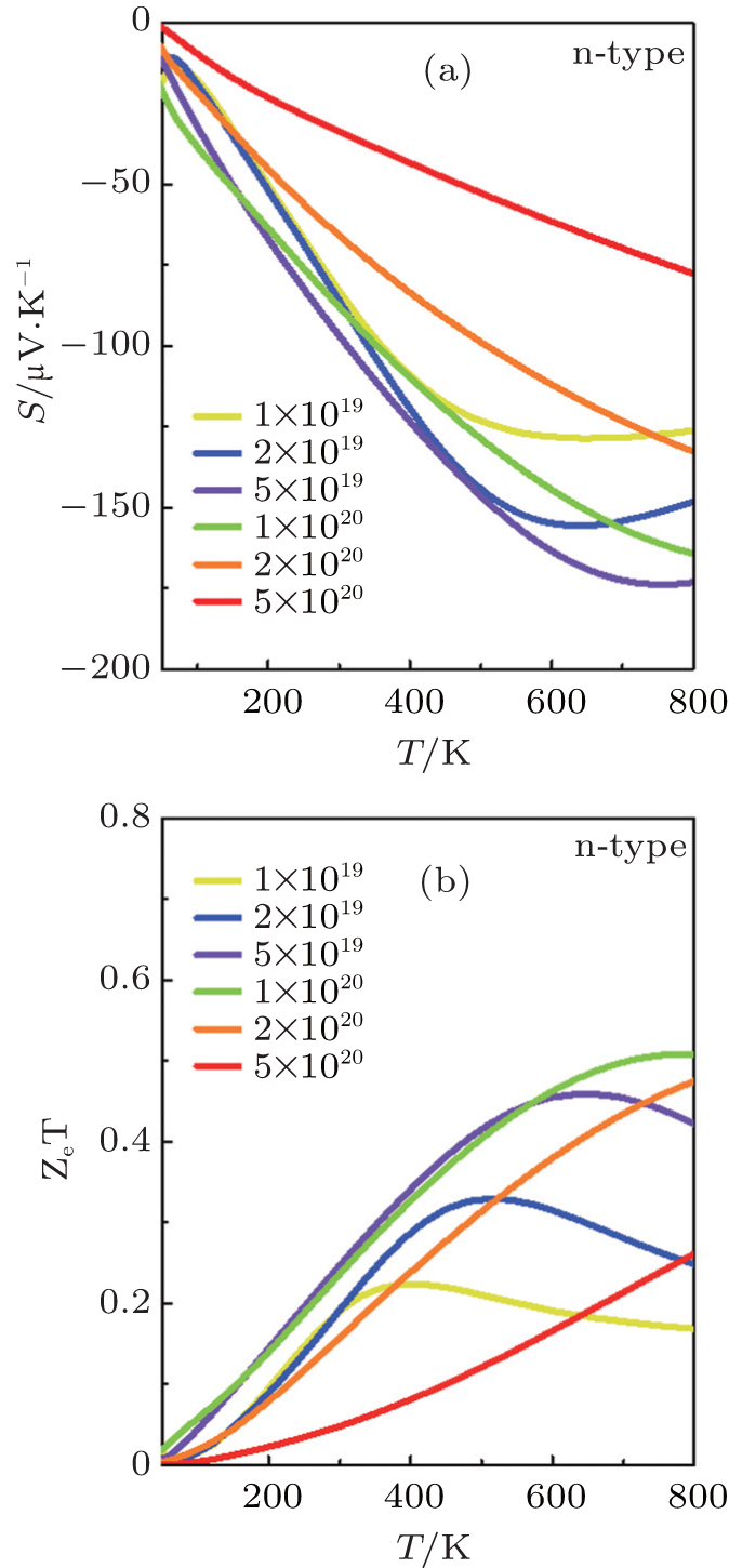
In order to investigate the TE properties of Cd 3 As 2 with different carrier densities, we calculate the Seebeck coefficient S based on the electronic structure by the semi-classical Boltzmann theory. The rigid-band approach is used to research how the thermoelectric performance depends on the doping level. Since the intrinsic Cd 3 As 2 is an n-type material in the experiments, we first calculate S as a function of the temperature at different n-type carrier concentrations (Fig. 5(a) ). The calculated Seebeck coefficient S has different trends as a function of the temperature at various concentrations. At the electron concentration of the undoped Cd 3 As 2 ( n ∼ 10 19 cm −3 ), the calculated absolute value of S matches the experimental results nicely below 400 K (Figs. 5(a) and 3(b) ), indicating that the semi-classical Boltzmann theory is a good tool to describe the transport properties of Cd 3 As 2 . As the doping level is increased, the maximum of the calculated S increases to the optimum 170 μV·K −1 with n = 5 × 10 19 cm −3 at 700 K, and then decreases. Meanwhile, the thermoelectric figure of merit from electron contribution (Z e T) is also estimated through the formula Z e T = S 2 σT / κ e , which is also called “maximum” thermoelectric figures of merit. The corresponding Z e T shares the similar tendency with S as a function of temperature (Fig. 5(b) ). Below 400 K, the Z e T value first increases then decreases roughly with the decrease of the electron concentration, in the same trend as the behavior of ZT of the Cr-doped sample (refer to Fig. 4(c) ). The critical temperature corresponding to the optimum merit Z e T becomes smaller as the carrier density decreases, which is also in good agreement with the Cr-doped samples. From Fig. 5(b) , the maximum optimum merit Z e T is found to be about 0.5 at T = 700 K with n = 1 × 10 20 cm −3 .
Fig. 5. Calculated Seebeck coefficient and thermoelectric figure of merit from electron contribution at different doping concentrations and temperatures. (a) and (b) Temperature-dependent Seebeck coefficient and Z e T obtained from the theoretical calculations based on n-type Cd 3 As 2 with different electron concentrations, respectively.
5. Conclusion and perspectives
In conclusion, our work unveils the electrical and thermal transport properties of Cd 3 As 2 . Cd 3 As 2 possesses a high electron mobility of 1800 cm 2 ·V −1 ·s −1 and a low thermal conductivity of 4.17 W·m −1 ·K −1 along with a large PF of 1.58 mW·m −1 ·K −2 at room temperature, comparable to the commercially available bulk Bi 2 Te 3 and PbTe. Meanwhile, its TE parameters can be effectively modulated by the carrier doping as revealed by both the doping experiments and the theoretical calculations. After finishing this work, we became aware of two related works [ 22 , 26 ] suggesting that magnetic field can greatly enhance the electrical to thermal conductivity ratio and possible field-induced quantum critical point in Cd 3 As 2 . Combining their study, a significant increase in TE property is anticipated with optimized carrier density and external magnetic field. It is interesting to see if intrinsic magnetic order can replace the requirement of magnetic field. The rich physics along with the unexpected good TE performance reveals the high-mobility Dirac semimetal Cd 3 As 2 as a new type of TE materials that is worth further study.
Reference
1
Dresselhaus M Chen S G Tang M Y Yang R Lee G H Wang D Z Ren Z F Fleurial J P Gogna P 2007 Adv. Mater. 19 1043
Liu Z K Jiang J Zhou B Wang Z J Zhang Y Weng H M Prabhakaran D Mo S K Peng H Dudin P Kim T Hoesch M Fang Z Dai X Shen Z X Feng D L Hussain Z Chen Y L 2014 Nat. Mater. 13 677
11
Zhang C Zhang E Liu Y Chen Z G Liang S Cao J Yuan X Tang L Li Q Gu T Wu Y Zou J Xiu F 2015 arXiv:1504.07698[cond-mat.mtrl-sci]
12
Jeon S Zhou B B Gyenis A Feldman B E Kimchi I Potter A C Gibson Q D Cava R J Vishwanath A Yazdani A 2014 Nat. Mater. 13 851
13
Neupane M Xu S Y Sankar R Alidoust N Bian G Liu C Belopolski I Chang T R Jeng H T Lin H 2014 Nat. Commun. 5 3786


 ]
]