†Corresponding author. E-mail: cjfu@pku.edu.cn
*Project supported by the National Natural Science Foundation of China (Grant No. 51076002), the National Basis Research Program of China (Grant No. 2013CA328900), and the Key Project of Complicated Electromagnetic Environment Laboratory of CAEP, China (Grant No. 2015E0-01-1).
Spectral and directional control of thermal emission based on excitation of confined electromagnetic resonant modes paves a viable way for the design and construction of microscale thermal emitters/absorbers. In this paper, we present numerical simulation results of the thermal radiative properties of a silicon carbide (SiC) thermal emitter/absorber composed of periodic microstructures. We illustrate different electromagnetic resonant modes which can be excited with the structure, such as surface phonon polaritons, magnetic polaritons and photonic crystal modes, and the process of radiation spectrum optimization based on a non-linear optimization algorithm. We show that the spectral and directional control of thermal emission/absorption can be efficiently achieved by adjusting the geometrical parameters of the structure. Moreover, the optimized spectrum is insensitive to 3% dimension modification.
The remarkable optical response of microstructures has made them a subject of growing interest from both a scientific and application point of view, such as extraordinary optical transmission, [1, 2] surface enhanced Raman scattering, [3, 4] enhanced near-field radiative heat transfer, [5, 6] solar cells, [7] and metamaterials.[8– 12] The advantage of using microstructures in the control of thermal radiation is that the confined electromagnetic resonant modes can be excited within the microstructures and thermal radiation from the microstructures can, by coupling with the resonant modes, exhibit novel spectral and directional selectivity feature.[13– 17]
Significant progress has been made in the design of thermal emitters/absorbers based on the excitation of electromagnetic resonant modes during the last decade. Depending on the purposes of different applications, many structures have been proposed to achieve promising feature of thermal emission, such as selective enhancement of emissivity in broad bandwidth and range of emission angle, [18– 21] or in contrast, in ultra narrow bandwidth and range of emission angle.[22– 24] Nevertheless, most of the work found in the literature considered selective enhancement of thermal emission based on a single electromagnetic resonant mode. Optimization methods have also been used to find the optimum geometrical configurations that result in the best emissivity/absorptivity distribution, [25– 29] such as particle swarm optimization and non-Newton optimization method. However, due to the limitation of these structures, the emissivity/absorptivity distribution cannot be flexibly tuned. Recently, investigation of controlled thermal radiation by coupled electromagnetic resonant modes has suggested a flexible way to design thermal emitters/absorbers made of periodic microstructures.[30]
In this paper we systematically demonstrate the selective emissivity/absorptivity characteristic of an emitter/absorber in the mid-infrared spectrum. The structure of this emitter/absorber was proposed because excitation and coupling of different electromagnetic resonant modes can be realized within the structure, resulting in greatly enhanced emissivity/absorptivity in a broader spectral range.[31] A non-linear optimization algorithm is applied to obtain the optimized emissivity spectrum in a specified spectral range by adjusting the geometrical parameters of the structure. For simplicity in analysis and computation efficiency, the structure that we analyzed has only one-dimensional periodicity and the related emissivity/absorptivity spectrum is limited for TM waves.
The microstructure of the emitter/absorber that we considered in this work is shown in Fig. 1, which is composed of a one-dimensional photonic crystal (PC) sandwiched by two one-dimensional periodic arrays of SiC strips. The top-sided SiC strips have width w1 = 3.0 μ m, period Λ g, 1 = 6.0 μ m, and depth dg, 1 = 1.0 μ m. The SiC film between the top SiC strips and the PC has thickness ds, 1 = 0.25 μ m. The bottom-sided SiC strips have width w2 = 1.5 μ m, period Λ g, 2 = 3.0 μ m, and depth dg, 2 = 1.0 μ m, and are set on another SiC film of thickness ds, 2 = 5 μ m. In our simulation, the dielectric function of SiC was described by a simple Lorentz model[32] as 

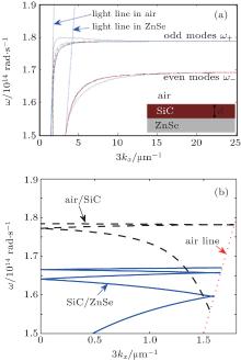
It is instructive to first address the resonant modes that are supported by the structure and responsible for the selective control of thermal emission/absorption. First of all, surface phonon polaritons (SPhPs) can be excited at the two interfaces of the air/SiC/ZnSe layered structure. If the air and ZnSe layers are assumed to be semi-infinite, then the dispersion relations of excited SPhPs are given by[35]

where ɛ 1 and ɛ 3 are the dielectric functions of the two semi-infinite layers, ɛ 2 and d are the dielectric function and thickness of the SiC slab, respectively. Fig. 2(a) shows the dispersion curves of the even and odd modes of SPhPs for the air/SiC/ZnSe structure with different values of the SiC slab thickness. It can be seen from Fig. 2(a) that when the SiC thickness is set larger than 1 μ m, the two dispersion curves are almost the same as those with d assumed infinity. Note that the dispersion curves for SPhPs excited at the air/SiC and the SiC/ZnSe interfaces have asymptotic values equal to ω = 1.79× 10¹⁴ rad/s and ω = 1.67× 10¹⁴ rad/s, respectively. One can see that the dispersion curves are located beyond the light cone, which means that there is a mismatch between the wave vectors of SPhPs and thermal radiating waves. However, if the thermal radiating waves are scattered by a grating, then the wave vector of the scattered waves may match with that of SPhPs as long as the following relation is fulfilled:[13]

where θ is the angle of emission, λ is the wavelength of thermal waves, and kx is the SPhP wave vector. Figure 2(b) shows the dispersion curves of SPhPs folded into the first Brillion zone of the grating with a period of 6 μ m, which is the same as that of the proposed structure. The result in Fig. 2(b) is helpful for us to analyze enhancement of thermal emission due to excitation of SPhPs.
 | Fig. 3. (a) Equivalent LC circuit model of the SiC strips. Dependence of the resonance frequency of MP on (b) grating depth and (c) grating gap width. |
Besides excitation of SPhPs, we also consider another resonant mode called diamagnetic response supported by the SiC strips, namely, magnetic polaritons (MPs). As shown in Fig. 3(a), the configuration of SiC strips can be treated as an equivalent LC circuit model to predict the resonant frequency of MPs, considering that the thickness of SiC strips is beyond the attenuation length of electromagnetic waves. The lumped element can be approximately given by[36]


where ɛ 0 = 8.854187× 10− 12 F/m is the vacuum permittivity; c1 = 0.55 accounts for the non-uniform charge distribution at the strip due to the induced electric currents; [36]l is the strip length in the y direction; μ 0 = 4π × 10− 7 V · s is the vacuum permeability; δ = λ /4π κ (κ the extinction coefficient of SiC) is the penetration depth; and, ɛ ′ is the real part of the dielectric function of SiC. Therefore, by setting the total impedance of the LC circuit equal to zero, in which condition the LC resonance is excited, we can obtain the resonance frequency of MPs. The dependence of MP resonance on geometrical parameters can be inferred from Eqs. (3) and (4) and are illustrated in Figs. 3(b) and 3(c), respectively. By adjusting the parameters of the grating we could get MPs excited at proper frequencies in the specified spectral band.
It should also be mentioned that unlike SPhPs and MPs, the PC-mode surface waves could be excited without gratings.[14] As an example, consider the structure studied in this work and assume that the filling factors of the top and bottom gratings are both equal to unity. Then, the PC is sandwiched by a SiC film of thickness 1.25 μ m on the top and another SiC film of thickness 7 μ m at the bottom, respectively. The emissivity of such a structure from the top surface is calculated and is shown in Fig. 4, in which two emissivity peaks can be clearly seen. These two peaks are the signature of PC-mode surface wave excitation. Note that if there is only one SiC film on the top or at the bottom of the PC, then the emissivity will exhibit only one peak at the same frequency, as illustrated in Fig. 4. Therefore, the two peaks are due to PC-mode surface waves excited on both ends of the PC, and their coupling results in the resonant mode splitting into two distinct ones.
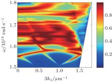
The emissivity/absorptivity of the emitter/absorber structure as a function of frequency and angle of emission (kx = ω sin θ /c) is depicted in Fig. 5, in which large area of emissivity/absorptivity enhancement can be clearly observed. The LC circuit model gives a prediction of ω = 1.77× 10¹⁴ rad/s for the resonance frequency of MPs. The high values of emissivity/absorptivity in the range of ω ≤ 1.68× 10¹⁴ rad/s are attributed to excitation of SPhPs located at SiC/ZnSe interfaces and PC modes between the SiC films and the PC, and interaction between these modes.[31] The excitation of these resonant modes and their interaction result in the wide direction (angle) as well as wide spectral band distribution of high emissivity/absorptivity, as shown in Fig. 5. By taking advantage of dependence of resonant modes on the structure’ s geometrical parameters, in the following study we show how to tune and optimize the emission/absorption feature based on a non-linear optimization algorithm.
In application, it is important to optimize the emissivity/absorptivity of the emitter/absorber in a given spectral and directional range. This, in light of the above analysis, amounts to control of the excitation of different electromagnetic resonant modes and their interaction. Since tuning the resonant modes’ frequencies can be performed by the flexible adjustment of the geometrical parameters of the microstructure, our optimization process is to find out a group of geometrical parameters with which the emissivity/absorptivity of the microstructure is optimized for specified purposes. From the above analysis, the geometrical parameters of the gratings such as Λ g, 1, dg, 1, f1, ds, 1, dg, 2, and f2 play important roles in the excitation of SPhPs and MPs. In addition, as will be shown in the following, introduction of defects in the PC can provide a promotion of resonant modes excited at bottom-sided grating. Therefore, three additional geometrical parameters a1, b, a1, t, and dcavity are also taken into account as the optimization arguments. Finally, the emissivity/absorptivity of the microstructure can be treated as a complicated function that depends on the geometrical parameters mentioned above.
The emissivity/absorptivity contours of the microstructure at normal direction are illustrated in Fig. 6 with the grating depth dg, 1 varying from 0 μ m to 2 μ m and the grating period Λ g, 1 from 2 μ m to 8 μ m. There exist many local maximum and minimum emissivity/absorptivity values in the searching space, which confirms the feasibility of optimization given a proper algorithm. The optimization process invariably relies upon characterization methods that must be robust as well as reliable. In this paper the Quasi– Newton method[37, 38] is used to find the geometry corresponding to the desired emissivity/absorptivity distribution, in which the Broyden– Fletcher– Goldfarb– Shanno (BFGS) scheme[39– 43] is chosen for the update of the Hessian matrix. In what follows we need to decide how to incorporate the practical constraints into the optimization scheme and to identify the objective function that represents the desired emissivity/absorptivity/distribution. For the first point, due to the physical and practical constraints, the searching space of the geometrical parameters is limited to certain ranges. One straightforward choice is to add additional positive costs in the objective function in case the geometrical parameters fall outside the desired boundaries. This adjustment of the objective function will not degrade the performance of the optimization algorithm. For the second point, the objective function of optimization should make the structure acquire the desired emissivity/absorptivity distribution, and at the same time it should be feasible for the BFGS non-Newton method. The choice of the objective function will be discussed in detail in the following.
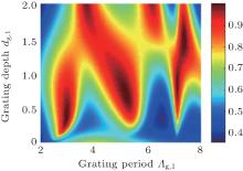 | Fig. 6. Emissivity/absorptivity contours as a function of the grating depth dg, 1 and the grating period Λ g, 1. |
At first we would conduct an optimization that makes the structure obtain the maximum average normal emissivity/absorptivity over the targeted spectral range. The average emissivity/absorptivity can be simply defined as

where θ = 0° represents normal direction, and ω max and ω min are the upper and lower bounds of the angular frequency, respectively. In the optimization procedure, minimizing the objective function should correspond to maximizing the average emissivity/absorptivity. For simplicity, we define the objective function as the inverse of average emissivity/absorptivity plus the additional positive costs and can be given by

where x is the vector of geometrical parameters discussed above and rewritten as

x(U) and x(L) are the upper and lower bounds of the searching space, respectively. Their values, between which resonant modes can be efficiently excited, are given as


Here β i and γ i represent the weight of the additional positive cost when searching point falls out of upper and lower bounds, respectively. The right choice of β i and γ i results in the maximum average normal emissivity/absorptivity in the optimization procedure. In other words, β i and γ i are called the penalty factors in the equivalent unconstrained optimization of the original problem. Thus, the factors should be large enough to make the convergence fast. In the present simulations, λ i = γ i = 100 (∀ 1 ≤ i ≤ 9) are empirically found to produce good results. M = 9 is the number of optimized arguments, and E(x) is the objective quantity and defined as


Therefore, the original problem is equivalent to finding min f (x) according to the theory of constraint optimization and Karush– Kuhn– Tucker conditions.[44]
Figure 7(a) illustrates the inverse cost function (1/f(x)) variation with the iteration steps, where the initial geometrical parameters are set as the original values shown in Fig. 1. It can be seen that an average emissivity/absorptivity of α avg = ɛ avg = 0.839 is obtained after 394 iterations. The corresponding geometry is

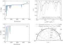 | Fig. 7. (a), (c) Evolution of inverse cost function (1/f (x)) as a function of iterations. (b), (d) The corresponding optimized results compared with those of the original structure. |
In Fig. 7(b) we can observe the emissivity/absorptivity distribution of the optimized structure in the specified frequency range, in which an improvement of 53.9% of the average emissivity/absorptivity is achieved for the optimized structure compared with that of the original. Mechanisms for the emissivity/absorptivity enhancement, related to the resonant modes discussed in Section 2, can be recognized. For example, the grating period Λ g, 1 in Eq. (12) is larger than its initial value, which results in the excitation of SPhPs at lower frequency, as can be inferred from Eq. (2). The optimized results balance the structure configuration for which resonant modes can be excited at most parts of the specified frequency range. While in Figs. 7(c) and 7(d), we perform an optimization of the average emissivity/absorptivity over the emission/absorption angle at a given frequency, which is similarly defined as

Following the same optimization procedure, very large values of the emissivity/absorptivity over the whole range of the emission/absorption angle can be obtained after 387 iterations. The most obvious improvement is that a great improvement of the emissivity/absorptivity at large angles is achieved. The average emissivity/absorptivity for the optimized structure has an improvement of 31.4% compared with that of the original structure. The corresponding optimized parameters are

The availability of a robust method for designing a thermal emitter/absorber system is essential, not only for broadband optimization but also for narrow band. In contrast to the work discussed above, we demonstrate below how to make an ultra-narrow band emitter/absorber, not only for frequency but also for direction. By utilizing the excitation and coupling of different resonant modes, the emissivity/absorptivity of the microstructure can be strongly enhanced at a particular frequency/direction and depressed otherwise, maximizing the emissivity/ absorptivity at a particular frequency or direction.
The Gauss function is commonly used to describe such a highly frequency or direction selective distribution. Thus, in the optimization procedure the objective quantity can be defined as the difference between the emissivity/absorptivity distribution and the Gauss distribution, which can be intuitively described as the integration of the variance over the whole frequency range or angle range,

where the Gauss function is defined as

with sd and sb being the center and width of the Gauss function, respectively. s = ω represents the frequency selective optimization and s = θ represents the direction selective optimization. The amplitude of the Gauss function is 4 instead of 1, since we want to increase the weight of sd in Eq. (15), which has been proved to be a good choice for optimization. To minimize the variance, the objective function can be defined as

and the same algorithm can be applied.
Figures 8(a) and 8(b) illustrate the optimized frequency selective results for the conditions of ω d = 1.62× 10¹⁴ rad/s, ω d = 1.71× 10¹⁴ rad/s, and ω d = 1.57× 10¹⁴ rad/s, respectively, with ω b = 0.01× 10¹⁴ rad/s and θ = 0° . One can see from Fig. 8(b) that the emissivity/absorptivity has a strong dependence on the frequency. The additional advantage of employing the Gauss function is that the width of the emissivity/absorptivity peak changes with the value of sb. The corresponding optimized parameters are

for ω d = 1.62× 10¹⁴ rad/s,

for ω d = 1.71× 10¹⁴ rad/s, and

for ω d = 1.57× 10¹⁴ rad/s, respectively.
Figures 8(c) and 8(d) show the optimized results of direction selective emissivity/absorptivity for the conditions of θ d = 0° , θ d = 45° , and θ d = 60° , respectively, with θ b = 5° and ω = 1.62× 10¹⁴ rad/s. One can clearly observe that the emissivity/absorptivity at θ d = 0° , θ d = 45° , and θ d = 60° is prominently enhanced while those at other angles are strongly suppressed, confirming the expected results. The corresponding optimized parameters are

for θ d = 45° ,

for θ d = 0° , and

for θ d = 60° , respectively.
By referring to the optimized results of θ d = 0° , we can observe an interesting phenomenon that the filling factor of the top-sided grating is equal to 1. It is worth noting that in the case of f1 = 1 there is no grating on the top side and the only resonant mode supported is the PC-mode surface wave.[14]
In what follows we will analyze the sensitivity of the structure to the possible imperfection during real micro/nano fabrications and the algorithm to the variation of the initial geometrical parameters, respectively. In Figs. 9(a) and 9(b), ± 3% perturbations are added to the optimized parameters of Eq. (12) and (14), respectively, and other settings are kept unchanged. It can be seen that the results with perturbation do not differ strongly from the original optimized ones, both for the spectral and directional distributions.
 | Fig. 9. Emissivity/absorptivity spectral distribution (a) and directional distribution with fabrication tolerances of the geometrical parameters (b). |
It should be noted that the quasi-Newton method is essentially deterministic in nature and is very likely to become trapped in local minima instead of global minima. In the optimization procedure over the specified frequency range, the initial values of the geometrical parameters are thought to be close to those corresponding to the global minimum point considering that the excited electromagnetic modes can improve the performance. In what follows we will conduct another two optimization procedures over the specified frequency range with different initial values of the geometrical parameters from the originals. Two perturbations are added to the initial values and they are defined as

and

and the other settings of the optimizations are kept unchanged. A comparison of the results is shown in Fig. 10, which indicates that the optimization with perturbation x″ finds an alternative set of optimized values that produce almost the same result as with those in Eq. (14), while those with x′ are likely trapped in a local extremum. The solid curve shows that the SPhP modes do not contribute so much as that of other two curves. The comparison implies that the initial geometrical parameters should be chosen at which the electromagnetic modes are efficiently excited, which can improve the quality of the optimized result.
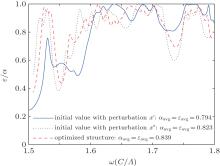 | Fig. 10. Comparison of optimized results for three sets of initial values of the geometrical parameters. |
In this work we have conducted numerical simulations on spectral and directional selectivity of thermal radiation from a microstructure composed of a PC sandwiched by two SiC gratings. Through analyzing the electromagnetic resonant modes associated with the selective thermal radiation and dependence of their resonance frequencies on the geometrical parameters of the structure, a non-linear optimization algorithm was employed to optimize the emission/absorption distribution in a certain range of wavelengths or angles of emission or absorption by adjusting the geometrical parameters of the structure. We successfully achieved different emissivity/absorptivity distributions, such as broadband, wide angle, narrowband and narrow angle enhancement of the emission/absorption, by defining different objective functions in the optimization procedures. The optimized structure is also shown to be insensitive to the imperfection introduced as a perturbation to the optimized parameters. Finally, this design and optimization strategy can be easily extended to three-dimensional periodic structures, which paves new pathways towards the efficient design and optimization of microstructures for selective control of thermal radiation.
| 1 |
|
| 2 |
|
| 3 |
|
| 4 |
|
| 5 |
|
| 6 |
|
| 7 |
|
| 8 |
|
| 9 |
|
| 10 |
|
| 11 |
|
| 12 |
|
| 13 |
|
| 14 |
|
| 15 |
|
| 16 |
|
| 17 |
|
| 18 |
|
| 19 |
|
| 20 |
|
| 21 |
|
| 22 |
|
| 23 |
|
| 24 |
|
| 25 |
|
| 26 |
|
| 27 |
|
| 28 |
|
| 29 |
|
| 30 |
|
| 31 |
|
| 32 |
|
| 33 |
|
| 34 |
|
| 35 |
|
| 36 |
|
| 37 |
|
| 38 |
|
| 39 |
|
| 40 |
|
| 41 |
|
| 42 |
|
| 43 |
|
| 44 |
|


