

Silicon nanowire formed via shallow anisotropic etching Si-ash-trimming for specific DNA and electrochemical detection
[Adam Tijjania)†  , HAshim U.
a)‡ , Dhahi Th S.b)§ ]
, HAshim U., Dhahi Th S.]
|
|


†Corresponding author. E-mail: tijjaniadam@yahoo.com
‡E-mail: uda@unimap.edu.my
§E-mail: Sthikra@yahoo.com
A functionalized silicon nanowire field-effect transistor (SiNW FET) was fabricated to detect single molecules in the pM range to detect disease at the early stage with a sensitive, robust, and inexpensive method with the ability to provide specific and reliable data. The device was designed and fabricated by indented ash trimming via shallow anisotropic etching. The approach is a simple and low-cost technique that is compatible with the current commercial semiconductor standard CMOS process without an expensive deep reactive ion etcher. Specific electric changes were observed for DNA sensing when the nanowire surface was modified with a complementary captured DNA probe and target DNA through an organic linker (–OCH2CH3) using organofunctional alkoxysilanes (3-aminopropyl) triethoxysilane (APTES). With this surface modification, a single specific target molecule can be detected. The simplicity of the sensing domain makes it feasible to miniaturize it for the development of a cancer detection kit, facilitating its use in both clinical and non-clinical environments to allow non-expert interpretation. With its novel electric response and potential for mass commercial fabrication, this biosensor can be developed to become a portable/point of care biosensor for both field and diagnostic applications.
The advance of nanotechnology has led to the development of large novel electronic devices with applications ranging through the physical, chemical, biological, and agricultural disciplines. Semiconductor silicon nanowires field effect transistor (SiWNs-FET) biosensors is an active area of research as they have been shown to be capable of detecting single molecule binding.[1– 4] If a low-cost and simple fabrication process can be devised, these sensors have great potential for different applications in point-of-care and other portable electronic devices; however, the potential of electrochemical transistors has been extended well beyond biosensors.[5, 6] The unprecedented sensitivity of the devices was obtained because of direct interaction between the internal electrical behavior of the nanowire and the short range electrostatic/electrochemical forces generated by molecules.[7– 10] The biosensors involve molecular scale interactions that significantly increase the complexity of the system, introducing new dynamics on various length and timescales which require great effort to understand.[11, 12] However, silicon nanowire biosensors are currently poorly understood and the precise mechanism of SiNW FETs is still not fully explored.[13– 16] The problem associated with this device is poor construction, which affects a range of factors, such as nanowire size and surface composition.[1, 17, 18] Due to the complexity of the device, many of the previous attempts to make nanowire SiNW-FETs have used very costly approaches to fabricate the devices and in terms of characterization, used only the way the signal changes based on the charge on the biomolecule and the doping of the nanowire to increase the conductivity.[19– 23] Previously, researchers attempted to use a biosensor for detecting a cancer tumor. However, all were used for general detection of molecular species but not explicit detection of a specific one. Thus, the present research attempts to bridge this gap in trying to detect a specific single molecule (DNA single strand) because at the early stage of disease, viruses have not spread or multiplied, making it very difficult for current devices to detect such a profile, and the early detection of diseases has tremendous impact and greatly increases the chances for accurate and successful treatment of any life threatening diseases.[23– 25] The early detection effort can be grouped into major management components that education to promote early diagnosis and screening and recognizing possible warning signs of potential risk and taking prompt action help early diagnosis and standardize the level of the disease. Increased awareness of possible warning signs of disease such as cancer, among physicians, nurses and other health care providers, as well as among the general public, can have a great impact on disease care. Some early signs of cancer include lumps, sores that fail to heal, abnormal bleeding, persistent indigestion, and chronic hoarseness.[1, 2, 26, 27]
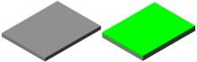
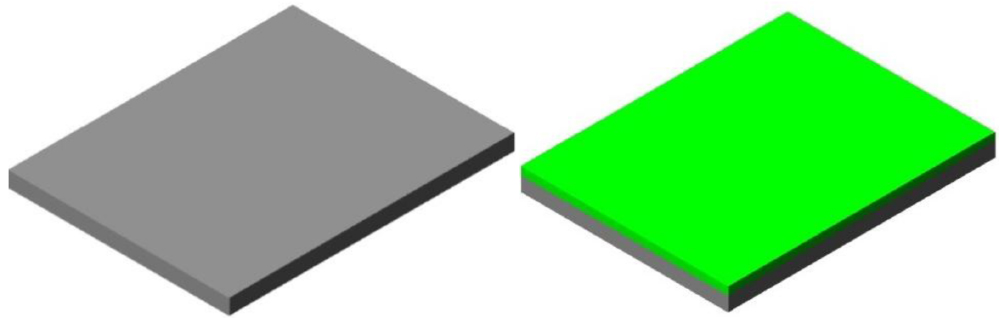
A 5-inch (1 inch = 2.54 cm) p-type silicon-on-insulator (SOI) and photoresist (PR), is coated with a thickness of 400 nm. After the exposure and development, a resist pattern between 3 μ m– 5 μ m was obtained. An oxygen plasma screen was used to reduce the size of the PR to 1-μ m patterns, and buffered oxide etching coupled with high temperature oxidation furnace were used to indent. Followed by trimming, the 1-μ m wire is thinned down to 20 nm by dry thermal oxidation coupled with 10:1 buffered oxide etchant (BOE). The Au interconnection is photolithographically defined and Au is deposited after dry etching of the last trimming stage followed a lift-off process. Then, the sample is pre-treated using ultra-thin titanium (Ti) to form an Ohmic contact between the silicon nanowire and gold pads. The process is as follows: the trimming process followed by using plasma processes to obtain the required nano sizes. This is done by growing oxide on the surface of a micro-size wire, which consumes polysilicon to form silicon oxide, and the oxide is later etched away. The thickness of the polysilicon consumed depends on the total penetration of the oxide, and this is controlled and limited by movement of oxygen through the oxide– silicon interface. The fabrication was done on p-type prime silicon wafer as a base material. The diameter of 100 mm or 4-inch p-type 〈 100〉 silicon wafer with the sensitivities of 0.005 Ω · cm– 1 Ω · cm and thickness about 525 ± 25 μ m is chosen for this research work. The sample preparation starts with a cleaning process. The silicon wafer was cleaned using standard cleaning (SC) or RCA and a buffered oxide etch (BOE) solution. There are four steps of the procedure for wafer cleaning. First, the wafer was dipped into RCA 1 at 70 ° C to 80 ° C for 10 minutes. Then, the wafer was dipped into the BOE solution for 10 s to 15 s to remove native oxide. After that, the wafer was dipped into the RCA 2 solution for 10 min to 15 min while the solution was heated to 75 ° C to 80 ° C. Then the wafer was rinsed in DI water or distilled water. Finally, the wafer was dried by blowing with spin dry. Initially, the top silicon layer was thinned to 200 nm by thermal oxidation growth. This layer is used for better adhesion of the resist layer during the resist coating process as well as a hard mask material for the silicon nanowires during the etching process. After cleaning and oxidation, the wafer was cut into small pieces, 2 cm by 1 cm, using a diamond saw. Now, the sample is ready for a resist spin coating process step and oxide layer (Fig. 1).
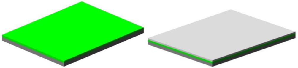
After the insulation process we deposited silicon on the insulated layer by a low-pressure CVD(LPCVD) process using silane (SiH4). The silicon is used for the material of nanowire fabrication (Fig. 2).
The process is followed by resist coating — a 270-nm thick layer of AZ-2000 resist is coated on the SiO2 layer for an AZ 2000 series resist mask. The choice of the resist thickness is based on a series of optimization processes conducted in a previous study. After the resist has been applied to the sample, it must undergo a soft bake. Then the coated sample is left for 30 minutes on the cool plate as a cooling step to achieve sample temperature control for uniform resist characteristics (Fig. 3).
 | Fig. 1. P-type silicon wafer with oxide layers. |
 | Fig. 2. Silicon deposition. |
 | Fig. 3. AZ-2000 resist coating on the SiO2 layer and soft bake of AZ-2000 resist coated sample. |
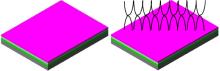
The resist coating process is as follows: the resist was spin-coated on silicon wafers with thickness of 0.3 μ m. The resist coated wafers were baked at 75 ° C for 3 minutes on a hotplate. The exposure process is shown in Fig. 4. Developing time was chosen to be at least twice the clearing time. Standard values were 20 s, 25 s, and 30 s, corresponding to the suitable exposure time. The exposure process followed and exposed to ultraviolet light through a mask after the exposure, the exposed part' s cross-link broke down and softened due to the photochemical reaction called photosolubilization and later dissolved by the developer while the unexposed part remained on the wafer surface. Processes are as follows: we used samples with the same viscosity throughout the experiments with different settings of the resist exposure and development. The exposure and development characteristics were measured using a high power microscope. Before the sample is subjected to hard bake, the exposed resist needs a certain time depending on the resist type and thickness, and for the purpose of this study we are using a positive photoresist with a thickness of 1 μ m and allowed it to stay for 3 min to outgas nitrogen (N2) formed during exposure. This will avoid bubbling (irregular developed structures) and foaming of the resist by thermally activated N2. Nitrogen preferentially accumulates near locations with inferior resist adhesion to the substrate, which can also be optimized with substrate pre-treatment by a sufficient soft bake. Photo mask and resist: reflection causes a number of problems for photo resist − reflection from the under laying substrate can cause a standing wave in the photoresist, or scattering from the underlying substrate may lead to photoresist exposure in an undesired area. The gap between the photo mask and the resist surface extends the diffraction pattern and therefore deteriorates the resolution; therefore, the exposure process was done with the photo mask tightly closed with the substrate to avoid possible trouble: (i) particles in the resist caused by either insufficient clean room conditions, contaminated substrates, or expired photoresist (ii) bubbles in the resist film caused during dispensing, or an insufficient delay time after refilling/diluting/moving the resist (iii) mask contamination by particles, or resist from previous exposure steps.
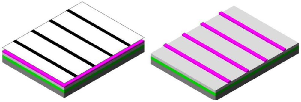 | Fig. 4. Exposed sample using mask aligner. |
After the exposure process in Fig. 4, the exposed sample was left for 10 minutes before it was unloaded from the mask aligner and then the development process proceeds. The resist exposed sample was developed in 30 s. Resist films were thoroughly rinsed with deionized (DI) water.
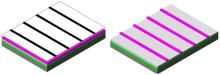
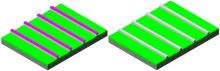
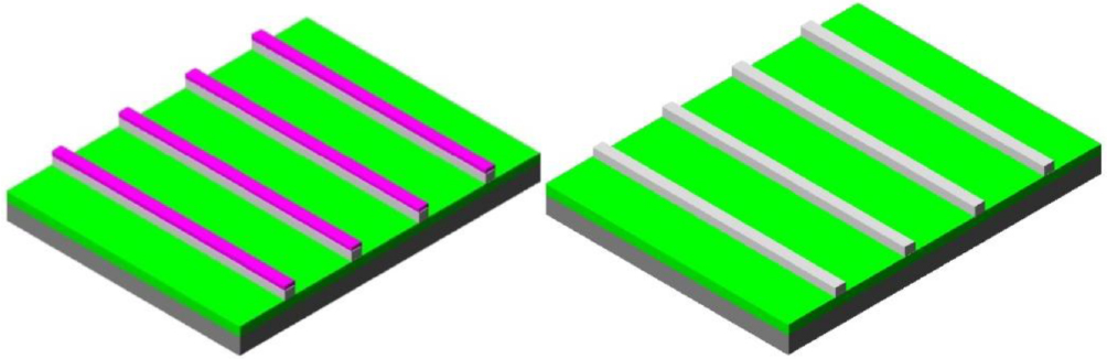 | Fig. 5. Etching process of SiO2. |
In order to form Si nanowires, the sample of SiO2 nanowires was loaded again into the prepared buffered solution to anisotropically etch the silicon for 1 minute. SiO2 nanowires were used as a hard mask for silicon etching. Next, the etch sample was dipped into a BOE solution for 4 minutes to remove all the unwanted SiO2. All the process flow of nanowires was completed after the BOE wet etch process (Fig. 5).
To make the oxide of silicon (SiO2) is the first step in modifying the nanowire surface and is one of the most important ingredients in a field effect transistor. SiO2 has excellent properties which makes it useful in every part of bio sensing.
Water (H2O) is passed on silicon (SiO2) in a furnace at 1000 ° C to form Si(OH)4 and the silicon nanowire surface containing large amounts of SiOH are hydroscopic and readily adsorbed ions from the biomolecule sample. The ions migrate through the oxide materials and silicon nanowire. This causes electrical changes under a bias. The ion is consumed as the strength of the electricity increases. This depends on the molecule concentration and this is the basis of the silicon-rich oxides as ion absorbers or barriers.
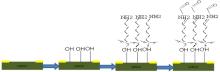
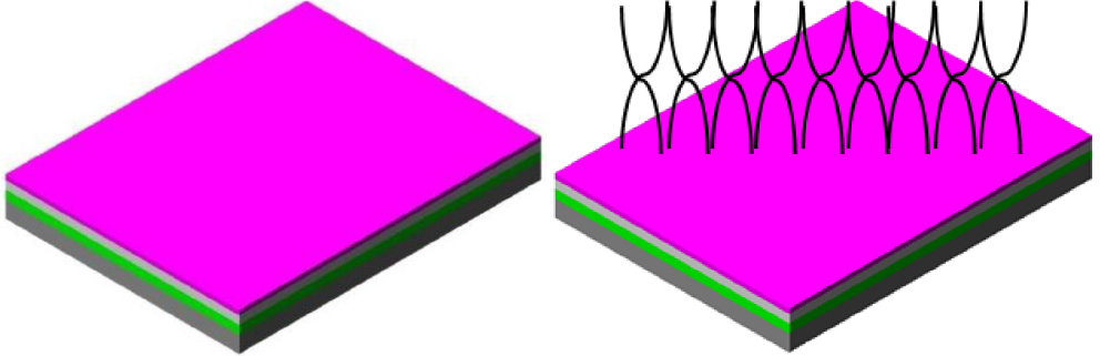
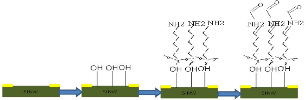 | Fig. 6. Surface functionalization of silicon nanowires (SiNWs) by 3-amino propyl triethoxysilane (APTES). |
An amine terminated surface monolayer can be obtained by using APTES and results in surface exposed − NHN2 (amine) groups that can be bioconjugated by using a proper coupling reagent like glutaraldehyde to produce a surface that is reactive toward amine groups that are present (Fig. 6). After the formation of (OH), the 3-APTES solution was coated to link glutaraldehyde. The next step is to attach the probe DNA, and a hybridization probe is a single part of DNA which is used in DNA samples to identify and detect the presence of nucleotide sequences (the DNA opposite target) that are complementary to the sequence in the probe; however, that could be mismatched or fully complementary. The probe thereby hybridizes to single-stranded nucleic acid whose base sequence allows probe-target base pairing due to the complementarity between the probe and the target. The process is as follows: the labeled DNA is first denatured (by heating or under alkaline conditions such as exposure to sodium hydroxide) into single stranded DNA (ssDNA-complementary) and then hybridized to the target ssDNA.
Figure 7 shows SEM images at the 5th etching step and 6th stage of the device etching. Note the trend of the reduction: oxidation at 1000 ° C consumes the silicon to a certain depth depending on the time and temperature, and the fundamental behind the reaction between oxygen and silicon is diffusive in nature, and the atomic level interaction between oxygen and silicon is also a diffusion process wherein the relatively open structure of silicon– oxygen molecules diffused through the growing SiO2. The oxidizing species are transported from the bulk gas to the gas/oxide interface with flux (where flux is the number of molecules crossing a unit area per unit time). The species are transported across the growing oxide toward the silicon surface with different flux and react at the Si/SiO2 interface with another flux.
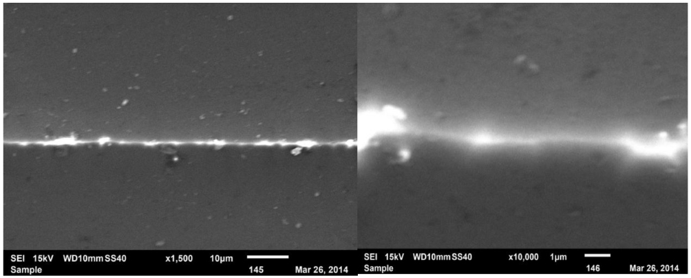 | Fig. 7. SEM image (a) 5th etching step and (b) 6th stage of the device etching. |
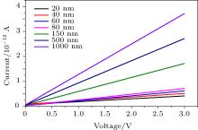
In order to characterize the trimming of the device through monitoring the conductance of the silicon of nanowires, the current– voltage (I– V) curve is obtained in the voltage range from 0 V to 3 V. The result of ash trimming is presented in Figs. 7 and 8. They show a comparison among the electrical characteristics of various wire widths during the wire trimming process. After the wire pattern is formed ≈ 1 μ m, the trimming process via oxidation furnace follows. It shows the current value decrease with the wire thickness decreasing, indicating the resistance is increasing from ≈ 1 μ m to ≈ 20 nm; the 200-nm wire is thinned down to 20 nm after 6 steps by dry thermal oxidation coupled with 10:1 buffered oxide etchant (BOE). The Au interconnection is photolithographically defined and Au is deposited after dry etching of the last trimming stage followed by a lift-off process. Then, the sample is pre-treated using ultra-thin titanium (Ti) to form an Ohmic contact between the silicon nanowire and the gold pads. Once the trimming process has been completed, the device current– voltage (I– V) characteristic is then measured by using a Keithley 4200 Semiconductor Parameter Analyzer. During this process, a measurement process was set up: a typical I– V measurement setting is employed on the two fabricated NW devices by supplying voltages to the source (S) region and obtains the output current at the drain (D) region shown in Fig. 8 as well.
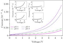
pH detection was conducted to determine the capability of the device, wherein we subjected it to 4 pH values, and to achieve this, the device was operated based on the principle of a field effect transistor (FET). Since the surface of the device is hole-dominated (p-type material), it is quite convenient to determine to the pH values, and in order to strengthen its response we further treated the surface of the silicon nanowire by a process called protonation in higher pH fluid, and mobile carriers (holes) drop due to the electrostatic interaction between the charge of the nanowire at its outer surface and the mobile carriers inside. With the same approach, the surface of silicon nanowire is deprotonated in lower pH liquid and the mobile carriers are depleted at the inner surface of silicon nanowire. When tested with pH at 4, 6, 8, and 9 (Fig. 9), p-type Si nanowire devices modified in this way exhibit stepwise increases in conductance as the pH of the solution increases.
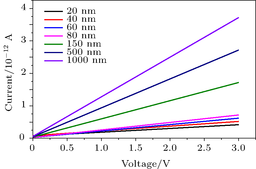 | Fig. 8. I– V curve of the wire trimming trend. |
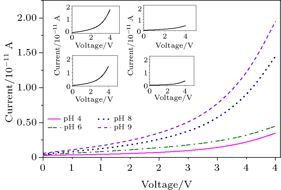 | Fig. 9. Device pH response conducted on four different pH values. |
As can be seen above, conductance increases linearly with increasing pH, resulting from protonation/deprotonation over different pH ranges. On the other hand, the increase in conductance with increasing pH is consistent with a decrease (increase) of the surface positive (negative) charge, which ‘ turns on’ the p-type FET via the accumulation of carriers.
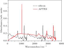
For the detection of bio-species, APTES is coated for perfect attachment of the DNA capture probe, and figure 10 shows the recorded absorbance UV/Vis/spectra of the silicon and APTES. The APTES spectrum has a clear, broad, strong peak at around 1000 cm− 1. The absorbance of the silicon appears at ≈ 650 cm− 1 and decreases across most of the spectral region ≈ 2500 and ≈ 2750 indicating lower absorbance. However, the final product, APTES on silicon, shows higher absorbance in the entire spectral region. It is quite obvious that the optical properties of silicon have been changed after coating by APTES. A weak absorbance peak in the UV frequency region still exists, confirming that the silicon bonds exist. The overall results of the recorded UV/Vis/spectra of samples indicate that in the silicon and APTES structure is clearly dominant.
 | Fig. 10. Absorbance UV/Vis/NIR spectra of the two materials (silicon and APTES). |
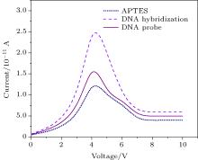
The DNA cell was detected by measuring the conductance of the SiNW when the target biomolecules (5′ CTA CGG TCA TCA CAA ATC TAC TAT CAG-3′ ) bind to the receptor (5′ -CTG ATA GTA GAT TTG TGA TGA CCG TAG AAA). First, we observed the characteristics of the SiNWs by measuring the current– voltage characterization. In Fig. 11, the responses were observed as the samples are dropped for measurement. However, it is known that the response of the system is affected by factors such as nanowire size and surface composition. The organic components (– OCH2CH3) using organofunctional alkoxysilanes (3-aminopropyl) triethoxysilane (APTES). The receptor ss-DNA interacts with the sensor platform, resulting in an increase in the current being measured due to the field created across the silicon nanowire by partial charge. This sensor allows the detection ss-DNA cells at concentrations as low as a single cell, and a device can be prepared to be able to evaluate several samples at the same time. Many cells could be evaluated in a rapid way. The simplicity of the sensing domain makes it feasible to miniaturize it for the development of point-of-care kits, facilitating its use in both clinical and non-clinical environments. With its novel electric response and potential for mass commercial fabrication, such a silicon-based biosensor can be developed to become a portable/point of care biosensor for both field and diagnostic application

The response of the device is 95%; therefore the device response shows it can detect as low as 1 nmole/L-DNA, which qualifies it to be the best candidate ever for detection of cancer and cancer-related diseases that need a very sensitive device to detect at the early stages. We demonstrate a novel and highly sensitive rapid detection kit for cancer tumors. From the results, the change in conductance of the nanowire due to the change in surface charge at the surface curve is nearly linear during wire trimming, to the partial charge on the surface of the nanowire. The study established that the device behaves like an FET transistor and modification in the surface charge, in turn, affects distribution of electrostatic potential throughout the nanowire. This change in electrostatic potential affects the conductance of the nanowire, which is detected as fluctuations in current when a voltage is applied at appropriate terminals of the NWFET. The device was tested using four different concentrations: 1 mole/L-DNA probe, 1 mole/L-DNA hybridization. The response was estimated to be 95%; hence the device response shows it can detect as low as 1 mole/L-DNA.
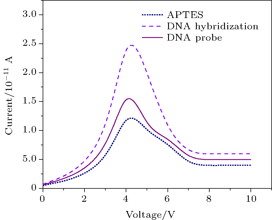 | Fig. 11. Sensing results for APTES, DNA probe, and DNA target hybridization. |
We developed a novel and highly sensitive biosensor. The change in electrostatic potential due to the concentration of the DNA affected the conductance of the nanowire, which was detected as fluctuations in current when a voltage is applied at appropriate terminals of the NWFET. The device was tested using three different samples: 1 mole/L-DNA probe, 1 mole/L-DNA mis-match, 1 mole/L-DNA complimentary, and the response was estimated to be 95%; hence the device response shows it can detect as low as 1 nmole/L-DNA. With its novel electric response and potential for mass commercial fabrication, such a silicon-based biosensor can be developed to become a portable/point of care biosensor for both field and diagnostic application, and we demonstrated a novel and highly sensitive rapid detection kit for cancer tumors. From the results, the change in conductance of the nanowire due to a change in surface charge at the surface curve is nearly linear during wire trimming, to the partial charge on the surface of the nanowire. The study established that the device behaves like an FET transistor, and modification in the surface charge, in turn, affects the distribution of electrostatic potential throughout the nanowire. This change in electrostatic potential affects the conductance of the nanowire, which was detected as fluctuations in current when a voltage is applied at appropriate terminals of the NWFET. The device was tested using four different concentrations: 1 mole/L-DNA probe, 1 mole/L-DNA. Target complimentary and the response was estimated to be 95%; hence the device response shows it can detect as low as 1 nmole/L-DNA.
The authors wish to thank Universiti Malaysia Perlis UniMAP and the Ministry of Higher Education Malaysia for giving the COE-MTUN grant to conduct this research in the Micro & Nano Fabrication Lab. Appreciation also goes to all the team members in the Institute of Nanoelectronic Engineering especially the nano structure lab on chip research group.
| 1 |
|
| 2 |
|
| 3 |
|
| 4 |
|
| 5 |
|
| 6 |
|
| 7 |
|
| 8 |
|
| 9 |
|
| 10 |
|
| 11 |
|
| 12 |
|
| 13 |
|
| 14 |
|
| 15 |
|
| 16 |
|
| 17 |
|
| 18 |
|
| 19 |
|
| 20 |
|
| 21 |
|
| 22 |
|
| 23 |
|
| 24 |
|
| 25 |
|
| 26 |
|
| 27 |
|