


Formation of two-dimensional electron gas at AlGaN/GaN heterostructure and the derivation of its sheet density expression*
[He Xiao-Guang, Zhao De-Gang† , Jiang De-Sheng]
, Jiang De-Sheng]
|
|


†Corresponding author. E-mail: dgzhao@red.semi.ac.cn
*Project supported by the National Natural Science Foundation of China (Grant Nos. 61377020, 61376089, 61223005, and 61176126) and the National Science Fund for Distinguished Young Scholars, China (Grant No. 60925017).
Models for calculating the sheet densities of two-dimensional electron gas (2DEG) induced by spontaneous and piezoelectric polarization in AlGaN/GaN, AlGaN/AlN/GaN, and GaN/AlGaN/GaN heterostructures are provided. The detailed derivation process of the expression of 2DEG sheet density is given. A longstanding confusion in a very widely cited formula is pointed out and its correct expression is analyzed in detail.
High electron mobility transistors (HEMTs) based on AlGaN/GaN heterostructures have been widely studied and have exhibited outstanding performances in high-power and high-frequency devices.[1] Unlike conventional HEMTs made of modulation-doped semiconductor heterostructures, no intentional doping is required to generate two-dimensional electron gas (2DEG) at the AlGaN/GaN interface.[2] The main problem that hinders the further development of AlGaN/GaN HEMT is a lack of understanding the origin of 2DEG. There is no doubt that the large interface charge density in this system is correlated to the spontaneous and piezoelectric polarization and the resulting high electric field in the AlGaN barrier layer, [3] but the source of the large quantity of electrons is controversial. Among several different theoretical models to explain this issue, the most widely accepted one is that the 2DEG originates from the donor states on the AlGaN surface.[4] However, some details of the process of the formation of 2DEG are still somewhat unclear.
Also, an accurate expression of the sheet carrier concentration of 2DEG ns is critical to the further development of AlGaN/GaN HEMTs. There is an important and very widely cited equation reported for calculating the 2DEG concentration ns[5] (see Eq. (4) in this article, which will be discussed later in more detail). However, according to our investigation, there is a serious confusion in the expression of this equation, especially about the term of polarization sheet charge density σ . In this widely cited equation, 2DEG is considered to be caused by the net polarization charge of AlGaN and GaN (i.e., σ pol = σ AlGaN − σ GaN). However, according to our research, 2DEG is induced by the polarization of the AlGaN layer, and the term σ GaN should not be added into the expression. Usually the term of polarization sheet charge density σ is regarded as a parameter to be determined, which means that the value of σ should be calculated by fitting to experiment results, rather than defined before fitting. So the different understanding of the meaning of σ will not affect the simulation results. However, a misconception or confusion of the expression may hamper the further understanding of the properties of AlGaN/GaN structure.
In this work, we carefully analyze the process of 2DEG formation and provide a possible physical picture of the AlGaN/GaN heterostructure. Also, a derivation of the 2DEG density expression is given in detail to prove the its validity that it is the right expression.
In many studies concerning 2DEG, the existence of 2DEG is regarded as an a priori assumption.[3, 6, 7] There is no doubt about the existence of 2DEG in AlGaN/GaN heterostructure, but being aware of the existence of 2DEG is not helpful for understanding the mechanism of its formation. By splitting the whole heterostructure into two independent parts, analyzing separately and finally assembling together, we can see clearer physical pictures of AlGaN/GaN heterostructure and the process of the formation of 2DEG. All structures discussed in this work are pseudomorphic heterostructures with Ga-face polarity.
The polarization effect of an AlGaN layer grown on a GaN buffer induces positive polarization charge at the AlGaN/GaN interface and negative polarization charge at the top of the AlGaN layer. Thus an electric field is formed within the AlGaN layer. It is reasonable to regard the AlGaN surface and the AlGaN/GaN interface as two infinite charged planes, as the thickness of the whole epilayer is just several μ m, which is very small in comparison to the lateral size of the substrate.
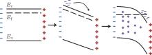
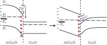
The formation of 2DEG of an AlGaN/GaN heterostructure with an n-doped AlGaN layer is easy to understand. In the AlGaN layer, the positive polarization charge at the AlGaN/GaN interface and the negative polarization charge at the top of the AlGaN layer induce an electric field and make the energy band (along with the Fermi level) tilt toward the interface. This situation is equal to applying a voltage to a piece of thin freestanding AlGaN film, in other words, a planar plate capacitor with AlGaN dielectric medium as shown in Fig. 1. Under the force of the electric field, conducting electrons (note that the AlGaN layer is n-doped) in AlGaN move to the positive electrode and accumulate there, leaving positive space charges in AlGaN, bending the energy band and making the Fermi level flat again. Also, the built-in electric field will reduce the whole electric field in the AlGaN layer and thus make the inclined energy band flatter. Once contacting GaN, electrons on the AlGaN side will flow into the GaN and form 2DEG, because the Fermi level of GaN is lower than that of AlGaN as shown in the left part of Fig. 2. This process will continue until the Fermi levels of AlGaN and GaN become equal to each other (the right part of Fig. 2).
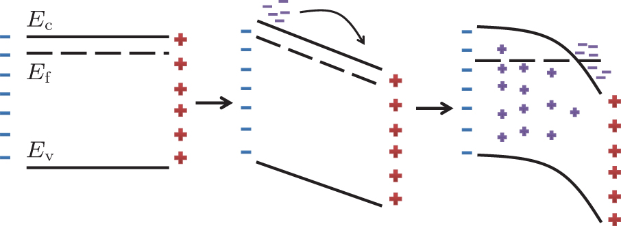 | Fig. 1. Energy band of n-doped freestanding AlGaN film (assuming the AlGaN layer to be under the same tensile strain as that when growing on GaN). Conductive electrons move under the polarization-induced electric field from one side to the other, thereby bending the energy band, and leaving fixed positive charges in the AlGaN layer. |
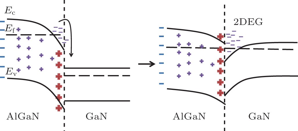 | Fig. 2. Energy band of an n-doped AlGaN/GaN heterostructure. When contacting a GaN layer, electrons will flow into the GaN side, accumulate at the interface and form 2DEG. |
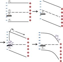
However, as for the case of undoped AlGaN, the situation is different. As shown in Fig. 3, in an undoped AlGaN/GaN heterostructure, few conductive electrons will move under the force of the electric field and the energy band will almost remain unchanged because of the lack of conductive electrons. When electrons contact the GaN, Fermi levels on the sides are close to each other and even the Fermi level of GaN may be higher, so very few or even no electrons will flow into the GaN side and no 2DEG will form. However, this does not accord with the fact that no intentional doping is required to generate 2DEG at the AlGaN/GaN interface.
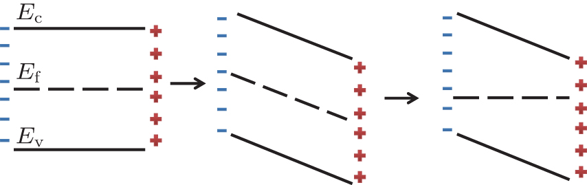 | Fig. 3. Energy band of undoped freestanding AlGaN on the assumption that the AlGaN layer is under the same tensile strain as that when growing on GaN. The polarization-induced electric field will not cause curvature of the energy band because of the lack of conductive electrons. |
Then where does the 2DEG come from? First, the 2DEG cannot come from the GaN buffer. The total polarization charge at the AlGaN/GaN interface can be divided into two parts. One part comes from AlGaN, and the other comes from GaN. The AlGaN part will have no effect on the GaN side because the negative polarization charge at the top of the AlGaN layer and the positive polarization charge at the interface forms a planar plate capacitor, which generates no electric field outside its two planes. Similarly, the GaN part, together with its counterpart at the bottom of the GaN layer, generates a uniform electric field pointing from the bottom of the GaN layer toward the AlGaN/GaN interface. This electric field will reduce the net electron density at the AlGaN/GaN interface, let alone form 2DEG. Second, the 2DEG cannot come from the body of the AlGaN barrier because there are few conductive electrons in undoped AlGaN as mentioned before.
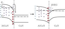
The formation of the 2DEG at the AlGaN/GaN interface can be well explained by assuming the existence of donor states on the AlGaN surface.[4] Figure 4 shows the energy band of a piece of freestanding AlGaN with surface donor states on the assumption that the AlGaN layer is under the same tensile strain as grown on GaN. If the AlGaN layer is thick enough, the Fermi level will reach the donor state level Es, and the electrons will be stimulated into the conductive band and swiped toward the other side by the force of the polarization-induced electric field. Once contacting with a GaN layer, electrons will flow into the GaN side because of the drop of the Fermi level. The electrons will accumulate at the interface and form 2DEG as shown in Fig. 5. The 2DEG and the ionized surface donor states will generate an electric field pointing from the interface to the surface and reduce the polarization field in the AlGaN layer.
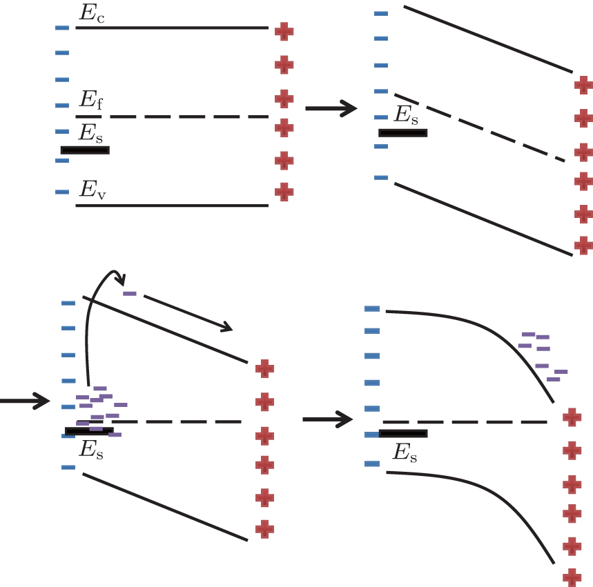 | Fig. 4. Energy band of undoped freestanding AlGaN (taking surface donor states into account). Electrons are stimulated into the conductive band and move under the force of the polarization-induced electric field. |
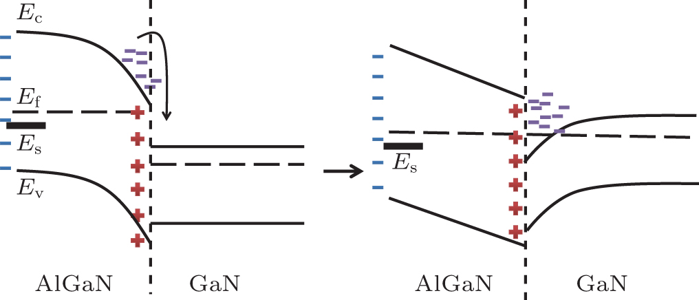 | Fig. 5. Energy band of an undoped AlGaN/GaN heterostructure. When contacting a GaN layer, electrons will flow into the GaN side, accumulate at the interface and form 2DEG. |
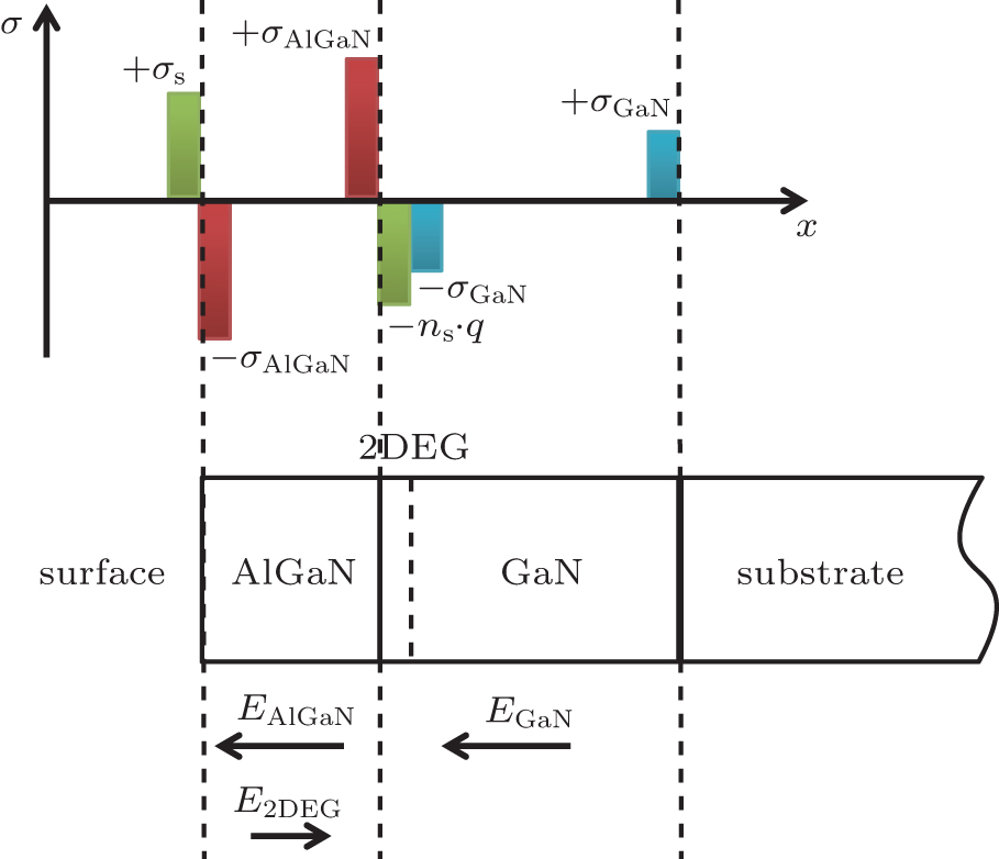
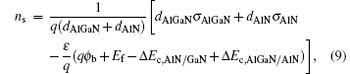
Based on the above discussion, a profile of the charge distribution of an AlGaN/GaN heterostructure is depicted in Fig. 6. There are three dipoles. First, ± σ AlGaN, the AlGaN polarization-induced charge; second, ± σ GaN, the GaN polarization-induced charge; third, the 2DEG and the ionized surface charge σ S. These three dipoles are equivalent to three planar plate capacitors C1, C2, and C3 respectively. Each of these capacitors only has a nonzero electric field between its two parallel planes and has no effect on electrons outside its inner body. The internal electric field intensity of a planar plate capacitor is given by E = σ /ε , where σ is the quantity of electric charges on opposite planes, ε is the dielectric constant of the dielectric medium of the capacitor. In the area where two or more pairs of charged planes overlap, the net electric field is the algebraic sum. Thus, the electric field intensity in the AlGaN layer is determined by the charges of C1 and C2, i.e., the AlGaN polarization-induced charge and the 2DEG:

where Δ VAlGaN is the potential drop across the conductive band of the AlGaN surface and the AlGaN/GaN interface (see Fig. 7), d is the thickness of the AlGaN layer, σ AlGaN is the sheet charge density that is induced by AlGaN polarization, ns is the sheet density of 2DEG, q is the electron charge, and ε is the dielectric constant of AlGaN. The potential drop Δ VAlGaN can be expressed as

where ϕ b is the surface barrier height, Ef is the Fermi level position with respect to the GaN conduction-band edge at the AlGaN/GaN interface, and Δ Ec is the conduction band discontinuity between GaN and AlGaN as shown in Fig. 7. Therefore, based on Eqs. (1) and (2), the sheet density of 2DEG can be expressed as

 | Fig. 6. Charge distribution profile of an AlGaN/GaN heterostructure. |
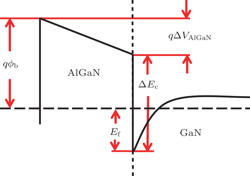 | Fig. 7. Conductive band diagram of an AlGaN/ GaN heterostructure. |
This equation is different from the one that has been widely cited[5]

where σ pol, the net polarization-induced charge density at the surface, is given by σ pol = σ AlGaN − σ GaN. However, as discussed before, σ GaN, the polarization charge induced by GaN has no effect on the potential drop of the AlGaN layer, and σ AlGaN is the contributor to the formation of 2DEG. According to our investigation, there was confusion in expressing the polarized sheet charge density σ pol in this equation, which was presented in a review article[5] and later widely cited by other research groups.[4, 6– 8] Actually, the expression in Ref. [5] was also cited from another paper, [9] which provides a 2DEG expression of the AlGaN/GaN heterostructure for the first time, to the best of our knowledge. In this article the authors did not take σ GaN into account and gave out an expression that was just the same as Eq. (3). For some unknown reason, in later citations, [4– 8]σ AlGaN was replaced by σ pol (equals σ AlGaN– σ GaN) in the ns expression. It is also not known why in another article[10] written by the authors of the same research group as that in Ref. [9], the first term of the expression of the net polarization sheet charge density at the interface was also changed into the same one that was presented in Ref. [5], i.e., σ pol, rather than σ AlGaN, was used in the ns expression. Unfortunately, there was no detailed derivation of this equation in these articles, so we actually do not know the real derivation process about how the authors obtained it. However, based on our analysis and discussion, we believe that the correct form of the expression should be the one as described by Eq. (3), i.e., the first term should be σ AlGaN, instead of σ pol.
Now an AlN interfacial layer[11] or a GaN cap layer[12] is often to added into the AlGaN/GaN HEMT structure to achieve a better performance. The expression of 2DEG sheet density ns of these two structures is easy to obtain based on the above discussion.
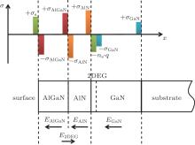
The profile of the charge distribution of an AlGaN/AlN/GaN heterostructure is shown in Fig. 8. The charges at the surface and interfaces can be regarded as four pairs of infinite charged planes with an equal quantity of heterogeneous charges. Each pair of planes only have a nonzero electric field within its two charged planes (E = σ /ε ) and have no effect on the outside region. In the area where two or more pairs of charged planes overlap, the electric field is the algebraic sum. Thus we can obtain the expression of the potential energy drop of the AlGaN layer and the AlN interfacial layer in a similar way


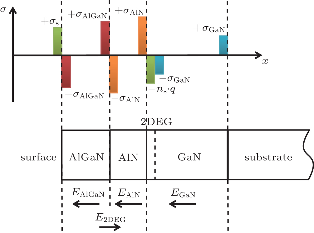 | Fig. 8. Charge distribution profile of an AlGaN/AlN/GaN heterostructure. |
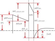
As shown in Fig. 9, the potential drop of the AlGaN layer across the surface and the AlGaN/AlN interface can be expressed as

where the effective conductive band gap Δ Ec, eff can be given as

where Δ Ec, a/b is the conductive band gap between material a and b.
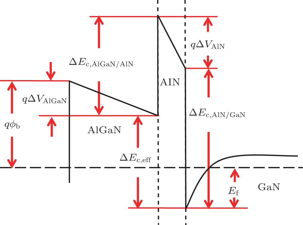 | Fig. 9. Conductive band diagram of an AlGaN/AlN/GaN heterostructure. |
From Eqs. (5)– (8), we can obtain the expression of the sheet density of 2DEG of AlGaN/AlN/GaN as
where ε is the dielectric constant of GaN, AlN, and AlGaN on the assumption that their dielectric constants are equal to each other, dAlGaN and dAlN are the thickness values of the AlGaN and AlN layer respectively, σ AlGaN and σ AlN are the polarization (including spontaneous and piezoelectric) charges induced by AlGaN and AlN layers, respectively.
Similarly, we can obtain the expression of the sheet density of 2DEG of GaN/AlGaN/GaN as follows:


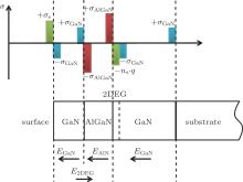
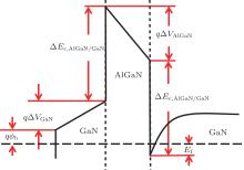
The charge distribution and the energy band figure are shown in Figs. 10 and 11.
 | Fig. 10. Charge distribution profile of a GaN/AlGaN/GaN heterostructure. |
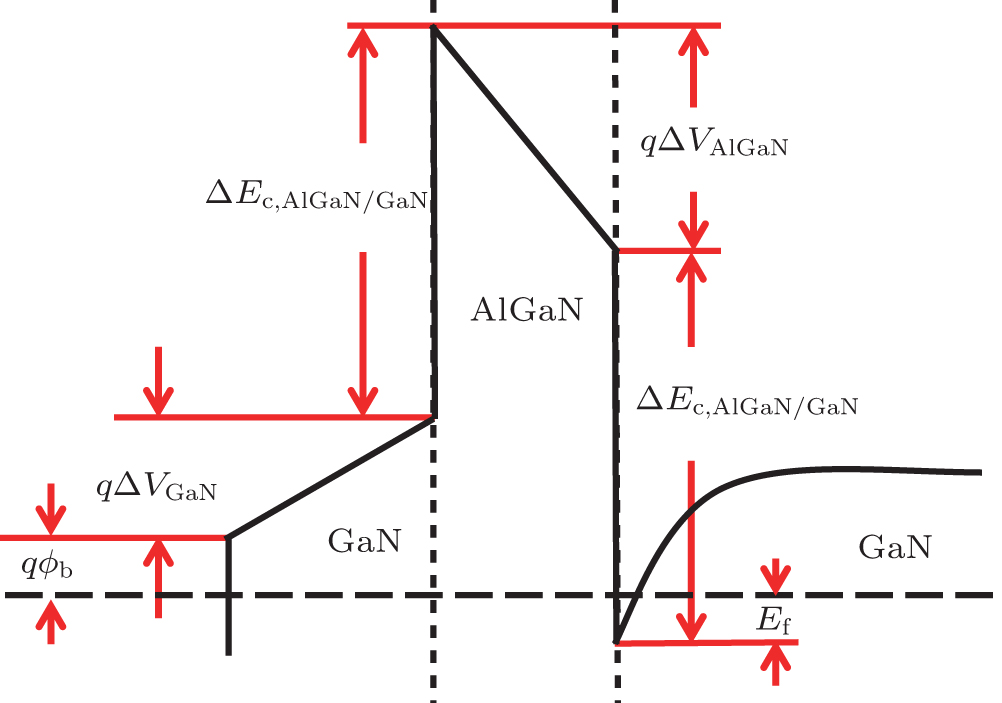 | Fig. 11. Conductive band diagram of a GaN/AlGaN/GaN heterostructure. |
In summary, according to the surface state model, we analyzed the formation of 2DEG in an AlGaN/GaN heterostructure. A detailed derivation of the expression of 2DEG sheet density of the AlGaN/GaN heterostructure is provided. A longstanding confusion about the expression of ns is analyzed in detail. It is proven that the polarization charge in the 2DEG formula should be σ AlGaN, the spontaneous and piezoelectric polarization-induced sheet charge of AlGaN, i.e., the net polarization charge at the AlGaN surface (σ AlGaN– σ GaN), instead of σ pol. The exact expressions of ns of AlGaN/AlN/GaN and GaN/AlGaN/GaN heterostructures are also derived in a corresponding way.
| 1 |
|
| 2 |
|
| 3 |
|
| 4 |
|
| 5 |
|
| 6 |
|
| 7 |
|
| 8 |
|
| 9 |
|
| 10 |
|
| 11 |
|
| 12 |
|