


Transparent ZnO/glass surface acoustic wave based high performance ultraviolet light sensors*
[Wang Wen-Boa) , Gu Hanga) , He Xing-Lia) , Xuan Wei-Penga) , Chen Jin-Kaia) , Wang Xiao-Zhia)†  , Luo Ji-Kui
a), b)‡ ]
, Luo Ji-Kui]
|
|

 , Luo Ji-Kui
†Corresponding author. E-mail: xw224@zju.edu.cn
‡Corresponding author. E-mail: Jackluo@zju.edu.cn
*Project supported by the National Natural Science Foundation of China (Grant Nos. 61274037 and 61301046) and the Research Fund for the Doctoral Program of Higher Education of China (Grant Nos. 20120101110031 and 20120101110054).
Surface acoustic wave (SAW) resonators are a type of ultraviolet (UV) light sensors with high sensitivity, and they have been extensively studied. Transparent SAW devices are very useful and can be developed into various sensors and microfluidics for sensing/monitoring and lab-on-chip applications. We report the fabrication of high sensitivity SAW UV sensors based on piezoelectric (PE) ZnO thin films deposited on glass substrates. The sensors were fabricated and their performances against the post-deposition annealing condition were investigated. It was found that the UV-light sensitivity is improved by more than one order of magnitude after annealing. The frequency response increases significantly and the response becomes much faster. The optimized devices also show a small temperature coefficient of frequency and excellent repeatability and stability, demonstrating its potential for UV-light sensing application.
Zinc oxide (ZnO) is a well-studied material, which has many desirable electrical, piezoelectric, and optical properties for various applications, such as light emitting diodes, [1] thin film transistors, [2] nano-generators, [3] solar cells, [4] acoustic devices, [5, 6] microfluidic actuators, [7] and sensors.[8, 9] As a direct band gap material with Eg ∼ 3.37 eV, it is sensitive to ultraviolet (UV) light. And it has shown excellent performance as a UV-light sensor.[10– 12] Among the UV sensors, the surface acoustic wave (SAW) based UV sensor is particular attractive due to its easy fabrication, good reproducibility, and high stability. Pang et al. developed a high sensitivity ZnO/LiTaO3 based SAW UV sensor, which delivered a ∼ 150 kHz resonant frequency shift with ∼ 350 μ W/cm2 UV illumination.[13] Wei et al. reported a ZnO SAW UV sensor on a silicon substrate, showing excellent sensing performance.[14] He et al. fabricated SAW UV sensors using ZnO films deposited on the polyimide substrate, and demonstrated their feasibility for wearable device applications.[15]
Transparent electronics is expected to become more and more important for modern optoelectronics, and there are growing interests and requirements in this field. Most of the developed SAW UV sensors were fabricated on bulk piezoelectric (PE) materials or thin films on crystalline substrates such as silicon and sapphire. They are all high cost and opaque materials, which limit their applications in transparent cases, such as flat panel displays, [16] window electronics, [17] and solar cells.[18] Owing to its merits of low cost, good transparency, and easy fabrication, the glass substrate based SAW UV sensor would be a good choice for transparent UV sensing. It can be made into components or as a sensor array on windows and screens to perform various sensing functions without blocking the visible light. We have developed a glass-based ZnO thin film SAW resonator, [19] and demonstrated the good performance of this type of device in UV sensing.[20] Since the quality of the ZnO thin film is one of the key issues for the UV sensors, improvement of the ZnO film quality will dramatically enhance the performance of the UV sensors. In this paper, we report the fabrication and evaluation of a new type of ZnO/glass based SAW UV sensors, and the effect of post-deposition thermal annealing on the performance.
ZnO thin films were deposited on 4 inch Corning 2318 glasses by direct current magnetron sputtering with the same optimized deposition conditions reported in the previous work, [20] except the deposition temperature which was set to 100 ° C in this work. After deposition, rapid thermal annealing (RTA) (RTP CT-100M, Premtek) was carried out for the wafers in a nitrogen atmosphere. The annealing temperature (TA) was set to be 200 ° C, 300 ° C, and 400 ° C for samples S2, S3, and S4, respectively (sample S1 is the as-deposited sample). The heating rate was ∼ 10 ° C/s, with a holding time of 10 min at the highest temperature, and all the samples were cooled down in a 1 L/min nitrogen flow. The aluminum interdigitated transducers (IDTs) of the SAW devices were fabricated with the conventional photolithography and lift-off process with a periodicity of 12 μ m (the wavelength λ ). More details of the devices can be found in our previous work.[20]
The SAW devices were characterized using an Agilent E5071C network analyzer, which was controlled by a LabVIEW-based measurement program. A UV lamp (ANUP 5252, Panasonic) with a 365 nm monochromator was used to deliver the UV light, and the light intensity was measured by a UV optometer (SUSS).
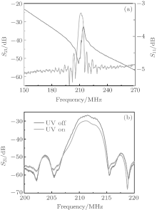
Figure 1 shows the schematic diagram and photos of the SAW UV light sensor. From Fig. 1(b), a good transparency of the devices can be seen, which is critical to transparent devices. Well-defined IDT electrodes are shown in Fig. 1(c). The reflection and transmission spectra are shown in Fig. 2(a) for the S4 device, which has the best performance among all the devices tested. A strong Rayleigh resonant peak with ∼ 30 dB amplitude can be observed at 211.5 MHz in the transmission spectrum. The detailed discussion of the SAW characteristics has been reported in Ref. [20]
 | Fig. 1. (a) Schematic diagram of a ZnO/glass SAW UV sensor device; (b) photo of the wafer; and (c) microscopy photo of IDTs. |
 | Fig. 2. (a) Transmission and reflection spectra and (b) UV response of the transmission spectrum (S21) of the S4 device. |
Owing to its ∼ 3.37 eV direct band gap, electron– hole pairs will be generated in ZnO when it is exposed to UV light. The photo generated holes will be recombined mainly with the excess electrons from the surface adsorbed oxygen.[21] Due to the surface recombination and the large absorption coefficient of ZnO, [22] the photo generated carriers are confined in the surface layer, which will increase the surface sheet conductivity σ S. This causes a change in both acoustic velocity and insertion loss as shown by the following equations:[13, 15, 23, 24]
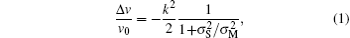

where v is the acoustic velocity, k2 is the electromechanical coefficient, σ M is the material relax conductivity, and Γ is the attenuation (insertion loss). With the increase of the surface sheet conductivity, the acoustic velocity decreases and the insertion loss increases. The UV response of the transmission spectrum of S4 is shown in Fig. 2(b). Under the UV light, the device shows a frequency shift about − 70 kHz and an insertion loss shift of ∼ 3 dB. Although both the variables can be used to characterize UV sensing, the shift of the insertion loss is less stable than that of the frequency, here we mainly discuss the frequency response of the SAW device to UV light.
The frequency response of the devices with different annealing conditions under a 7.6 mW/cm2 UV illumination is illustrated in Fig. 3. For the as-deposited device, ∼ 3 kHz frequency shift can be observed; S2, annealed at 200 ° C, shows little improvement in the frequency response; while for those with higher annealing temperatures (300 ° C and 400 ° C), the frequency shift becomes larger. S4 shows the best UV sensing performance with ∼ 70 kHz frequency shift, more than 20 times larger than that of the as-deposited device. The results demonstrate that the post-deposition annealing treatment can improve the performance of the ZnO SAW UV sensors significantly. Since the improvement in device characteristics for devices annealed at TA < 400 ° C is not significant, here we focus the investigation on the device annealed at 400 ° C. Although the performance of the S4 device is only comparable to that of the ZnO SAW UV sensors fabricated on bulk PE materials (e.g., LiNbO3 (∼ 100 kHz for 150 μ W/cm2, with ZnO nanowire), LiTaO3 (∼ 150 kHz for 3.10 mW/cm2, with ZnO thin film)), [13, 25] due to the merits of the glass substrate and transparency, it is convincing that the ZnO/glass based SAW UV sensor would be a good supplementary to the commercial UV sensors, especially for the transparent electronic applications.
 | Fig. 3. Frequency response of the SAW devices with different annealing temperatures. The UV light intensity is 7.6 mW/cm2. |
The resonant frequency shift versus temperature of the S4 device was measured and is shown in Fig. 4(a). It shows a good linear relationship. The temperature coefficient of frequency (TCF), defined as Δ f/(Δ T f0), can be calculated from the slope of the line. The value is − 31.6 ppm/K, which is consistent with the results obtained from the ZnO/glass SAW devices with Al-doped IDTs.[19] The low TCF could reduce the temperature influence to the UV sensor, improving the sensing performance of the sensor as compared with that of the LiNbO3 devices with high TCFs.[26]
 | Fig. 4. (a) Frequency as a function of temperature and (b) UV response at different temperature of the S4 device. The UV light intensity is 7.6 mW/cm2. |
To test the temperature stability of our devices, the UV light response of the S4 device at different temperatures was measured. At 20 ° C and 60 ° C, the device shows a similar ∼ 70 kHz frequency shift with no noticeable difference. However, when the temperature increases further to 90 ° C, the frequency shift decreases to ∼ 50 kHz, which is believed to be caused by the reduction of the surface adsorbed oxygen, [13] which reduces the surface recombination rate. For general transparent application such as on windows or screens, the working temperature would rarely go above 60 ° C, thus the results show that the ZnO/glass SAW UV sensors would be very reliable and stable.
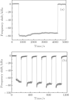
The stability and repeatability of the devices were further tested, and the results are shown in Fig. 5 for S4. To test the stability over a long period, UV illumination was applied to the device for 60 min with the temperature controlled within ± 1 ° C. From Fig. 5(a), it is clear that the frequency shift is almost constant during the long time UV illumination and the resonant frequency returns to its original value rapidly (within 10 s) once the UV light is switched off, showing a good stability of UV sensing. The response of the S4 device to cyclic UV illumination is illustrated in Fig. 5(b). When the light is switched on, the resonant frequency quickly decreases and vice versa. Within five cycles, the frequency shift and the response time remain unchanged, showing that the SAW UV sensors have excellent repeatability. It is interesting to note the difference between the initial and the subsequent responses. The frequency shift caused by the first on-light continues to increase with time slowly, while the response to the following on-light decreases with the increase in time. As reported in Ref. [16], devices S1– S3 were measured under the same condition and did not find such a phenomenon, implying that oxygen and water adsorption may not be the cause for this phenomenon. It is also noticed that this phenomenon has a response time of ∼ 750 s, much longer than that of the surface effect, thus it is mainly attributed to trapping and release of carriers to/from the deep level defects. The detailed discussion can be found in Ref. [20]. These results show that the UV sensors have the ability to work repeatedly for a long time under high intensity UV illumination, and have comparable performance to those of ZnO/LiNbO3 devices.[21] We also tested the devices after long time storage to see if they deteriorate or not. The devices maintain the same performance without any deterioration after storage in an unprotected environment for more than two months, implying superb reliability and stability of the sensors.
 | Fig. 5. Frequency response measurements to evaluate the UV sensor performance: (a) under long term (60 min) UV exposure, (b) under cyclic UV illumination. The S4 device is used for this test with an intensity of 7.6 mW/cm2. |
We have fabricated ZnO/glass SAW UV sensors, and investigated the effect of post-deposition annealing on their performance of UV sensing. The results showed that annealing at 400 ° C can significantly improve the UV sensitivity of the devices. The devices have a lower TCF and demonstrate excellent stability and repeatability. The optimized transparent sensors have a comparable performance to that made on bulk PE materials, demonstrate a great potential as low cost and transparent UV sensors.
The authors would like to acknowledge the Innovation Platform of Micro/Nanodevices and Integration System, Zhejiang University.
| 1 |
|
| 2 |
|
| 3 |
|
| 4 |
|
| 5 |
|
| 6 |
|
| 7 |
|
| 8 |
|
| 9 |
|
| 10 |
|
| 11 |
|
| 12 |
|
| 13 |
|
| 14 |
|
| 15 |
|
| 16 |
|
| 17 |
|
| 18 |
|
| 19 |
|
| 20 |
|
| 21 |
|
| 22 |
|
| 23 |
|
| 24 |
|
| 25 |
|
| 26 |
|