Zhao Yu-Kun, Li Yu-Feng, Huang Ya-Ping, Wang Hong, Su Xi-Lin, Ding Wen, Yun Feng. Efficiency droop suppression in GaN-based light-emitting diodes by chirped multiple quantum well structure at high current injection* . Chinese Physics B, 2015, 24(5): 056806
Permissions
Efficiency droop suppression in GaN-based light-emitting diodes by chirped multiple quantum well structure at high current injection*
Zhao Yu-Kuna),b), Li Yu-Fenga),b), Huang Ya-Pinga),b), Wang Honga),b), Su Xi-Linc), Ding Wena),b), Yun Fenga),b),c)†
Key Laboratory of Physical Electronics and Devices of Ministry of Education and Shaanxi Provincial Key Laboratory of Photonics & Information Technology, Xi’an Jiaotong University, Xi’an 710049, China
Solid-State Lighting Engineering Research Center, Xi’an Jiaotong University, Xi’an 710049, China
Shaanxi Supernova Lighting Technology Co. Ltd, Xi’an 710075, China
*Project suppored by the National High Technology Research and Development Program of China (Grant No. 2014AA032608), the Key Laboratory for Mechanical Behavior of Material of Xi’an Jiaotong University, China (Grant No. 20121201), and the Fundamental Research Funds for the Central Universities, China.
Abstract
Gallium nitride (GaN) based light-emitting diodes (LEDs) with chirped multiple quantum well (MQW) structures have been investigated experimentally and numerically in this paper. Compared to conventional LEDs with uniform quantum wells (QWs), LEDs with chirped MQW structures have better internal quantum efficiency (IQE) and carrier injection efficiency. The droop ratios of LEDs with chirped MQW structures show a remarkable improvement at 600 mA/mm2, reduced down from 28.6% (conventional uniform LEDs) to 23.7% (chirped MQWs-a) and 18.6% (chirped MQWs-b), respectively. Meanwhile, the peak IQE increases from 76.9% (uniform LEDs) to 83.7% (chirped MQWs-a) and 88.6% (chirped MQWs-b). The reservoir effect of chirped MQW structures is the significant reason as it could increase hole injection efficiency and radiative recombination. The leakage current and Auger recombination of chirped MQW structures can also be suppressed. Furthermore, the chirped MQWs-b structure with lower potential barriers can enhance the reservoir effect and obtain further improvement of the carrier injection efficiency and radiative recombination, as well as further suppressing efficiency droop.
Gallium nitride (GaN) based light-emitting diodes (LEDs), which represent a promising efficient solid-state lighting and display applications, have evoked great interest. Suffering from the internal quantum efficiency (IQE) droop with increasing injection current, LEDs deliver high efficiency thus far only at low current and low brightness.[1] The efficiency droop phenomenon is observed across a broad wavelength spectrum, from blue and green InGaN/GaN LEDs to deep ultraviolet (UV) AlGaN/AlN LEDs.[2, 3] Auger recombination, defects, inefficient injection and transportation of holes as well as carrier overflow out of the active region have been identified to be significant reasons for efficiency droop.[4– 6] To reduce the efficiency droop of GaN-based LEDs, several research works have been performed by improvement of large V-shape pits, epitaxy, the electron-blocking layer (EBL) design and package design, etc.[7– 11] Although significant steps forward have been made for the realization of high-brightness LEDs, it is still a big challenge to reduce the efficiency droop, especially at high injection current levels.
As the hole and electron injection and transport in LEDs with conventional uniform MQWs have been found to be ineffective and non-uniform in the active region, which leads to dominant carrier localization in only one QW, [12] chirped MQW structures could be another way to improve carrier injection and suppress efficiency droop. Chirped multi-quantum barriers have been utilized in EBL to reduce efficiency droop.[13] To improve the light output power (LOP), Chang et al. have utilized the chirped structures by inserting deeper QWs close to n-GaN and p-GaN.[14] However, based on their results, the efficiency droop effects become more serious. So far, limited papers reported about utilizing chirped structures in MQWs to suppress efficiency droop and improve hole injection efficiency.[15] In this work, we utilize two different chirped MQW structures to suppress efficiency droop and seek further promotion of hole-injection efficiency, as well as the improvement of LOP. A detailed and systematic investigation on the Auger and radiative recombination is also provided in order to study the suppression of efficiency droop.
2. Numerical parameters and models
All samples were grown on (0001)-oriented sapphire substrates by metal-organic chemical vapor deposition (MOCVD). During the epitaxial growth process, trimethylindium, trimethylgallium, trimethylaluminum, and ammonia were used as the source materials of In, Ga, Al, and N, respectively. An undoped GaN layer was grown, followed by 1.5-μ m-thick Si-doped n-GaN layers. The AlGaN EBL was grown followed by Mg-doped p-InAlGaN:Mg and a p-GaN:Mg (p-doping = 5 × 1019 cm− 3) layer. Lateral LED chips with ITO current spreading layer and Ni/Au contact metal were fabricated, and the size was 250 × 580 μ m2. The electroluminescence (EL) spectra of un-encapsulated LED chips were measured under different injection currents from 7 mA/mm2 to 600 mA/mm2 in a calibrated integrating sphere at room temperature.
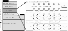
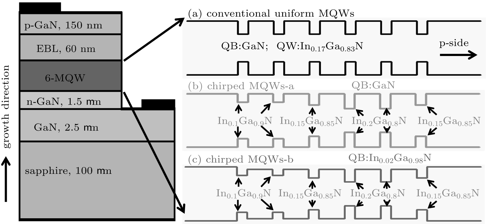
Prior to the experiments, we used the APSYS simulation program to investigate the optical and electrical properties of InGaN/GaN MQW LEDs by solving the Poisson equation, carrier transport equation, quantum mechanical wave equation, and photon rate equation, etc.[9] In this work, the effective mass for mean free path calculation has been introduced into the mechanism of direct flying-over in transport models, which could make the carrier distribution results more accurate. Simulations were carried out using a drift-diffusion approach with quantum-mechanical corrections. Figure 1 illustrates the structures of LEDs used for APSYS simulation work. The active region of conventional LED (uniform MQWs) consists of six 2.5-nm-thick In0.17Ga0.83N QWs, separated by seven 15-nm-thick GaN quantum barriers (QBs). To simplify the simulation, the operating temperature was set to be 300 K. In the simulation, the polarization densities of the built-in interface charges, which were produced by the spontaneous and piezoelectric polarization, were assumed to be 30% of the calculated values.[16]
Based on the structure with uniform QWs, the indium composition of the first QW in the first chirped MQW structure (chirped MQWs-a) was 10% (two QWs of In0.1Ga0.9N) close to the n-side and then changed to 15% (one QW of In0.15Ga0.85N), 20% (two QWs of In0.2Ga0.8N), and 15% (one QW of In0.15Ga0.85N) close to the p-side. As shown in Table 1, for the second chirped MQW structure (chirped MQWs-b), compared to chirped MQWs-a, the middle five quantum barriers are changed from GaN to In0.02Ga0.98N.
Table 1.
Table 1.
Table 1. Indium composition in InGaN/GaN MQW layers.
Layers (epitaxial direction)
1st QW
QB
2nd QW
QB
3rd QW
QB
4th QW
QB
5th QW
QB
6th QW
Uniform MQWs (In%)
17
0
17
0
17
0
17
0
17
0
17
Chirped MQWs-a (In%)
10
0
10
0
15
0
20
0
20
0
15
Chirped MQWs-b (In %)
10
2
10
2
15
2
20
2
20
2
15
Table 1. Indium composition in InGaN/GaN MQW layers.
Fig. 1. Schematic diagram plot of LEDs with (a) conventional uniform MQW structure, (b) chirped MQWs-a structure, and (c) chirped MQWs-b structure.
3. Results and discussion
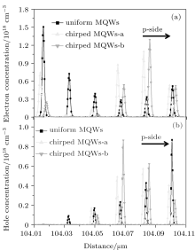
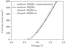
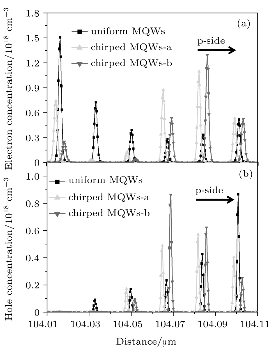
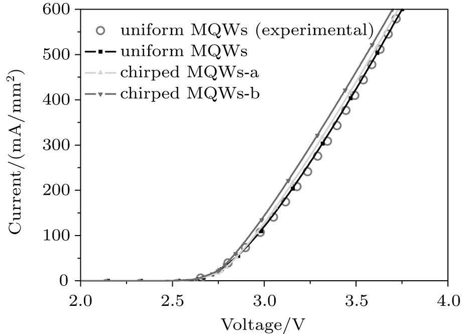
Figure 2 illustrates the electron and hole concentrations in the active region of the uniform and chirped MQW structure at an injection current of 600 mA/mm2. This figure shows that the electron concentration of uniform LEDs decreases significantly from the n-side to the p-side, as well as the hole concentration declines remarkably at the reversed orientation (from p-side to n-side), which indicates the carrier’ s inefficient injection and transport. For the electron and hole concentrations of chirped MQW structures distributed in the middle of the active region, they are higher than the uniform LEDs, especially in the fourth and fifth QWs (counted by the growth direction). It indicates that the two chirped MQW structures have better electron and hole injection efficiency and transportation. Figure 3 shows the current– voltage (I– V) characteristic curves of the uniform structure, chirped MQW-a, and chirped MQW-b. As illustrated in this figure, a good agreement is reached between the experimental data and simulated results for LEDs with uniform MQWs. Compared with LEDs with uniform MQWs, the turn on voltages of chirped MQW structures are reduced, especially for chiped MQWs-b, which may result from the enhanced electron and hole injection efficiency.
Fig. 3.I– V characteristics of the LEDs with uniform and chirped MQW structures.
Table 2.
Table 2.
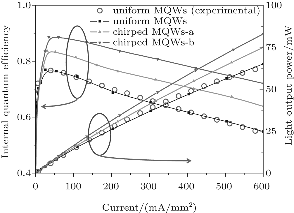
Table 2. Results for the IQE, droop ratio, and LOP.
Uniform MQWs (experimental)
Uniform MQWs
Chirped MQWs-a
Chirped MQWs-b
η /%
76.7
76.9
83.7
88.6
Q/%
29.2
28.6
23.7
18.6
LOP at 600 mA/mm2/mW
61.5
63.6
73.2
81.0
Table 2. Results for the IQE, droop ratio, and LOP.
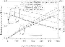
Figure 4 shows the IQE (η ) and LOP-current (L– I) characteristic curves of the uniform and chirped MQW structure. The droop ratio (Q) is defined and calculated as
where η 600 mA/mm2 and η max are the IQE at 600 mA/mm2 and the peak IQE, respectively. More details of the results are shown in Table 2.
As shown in Fig. 4 and Table 2, the experimental and simulation results of LEDs with uniform MQWs agree with each other, which reveals a good agreement between simulation models and LED samples for conventional LEDs. To some extent, based on the good fit, we has the confidence to model and analyse the chirped MQWs-a and MQWs-b structures. The uniform LED exhibits a serious droop ratio of 28.6% in Fig. 4, while the droop ratio of LEDs with chirped MQW structures shows a remarkable improvement, 23.7% for chirped MQWs-a and 18.6% for chirped MQWs-b. In addition, the maximum IQE increases from 76.9% (uniform LEDs) to 83.7% (MQWs-a), and 88.6% (chirped MQWs-b). Furthermore, the LOP of LEDs with chirped MQW structures increases from 63.6 mW (uniform MQWs) to 73.2 mW and 81.0 mW at 600 mA/mm2 for chirped MQWs-a and chirped MQWs-b, respectively. Compared to conventional uniform LEDs, the LOP is enhanced by 15.1% and 27.4%.
Fig. 4. IQE and L– I characteristics of LEDs with uniform and chirped MQW structures.
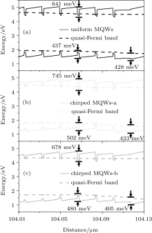
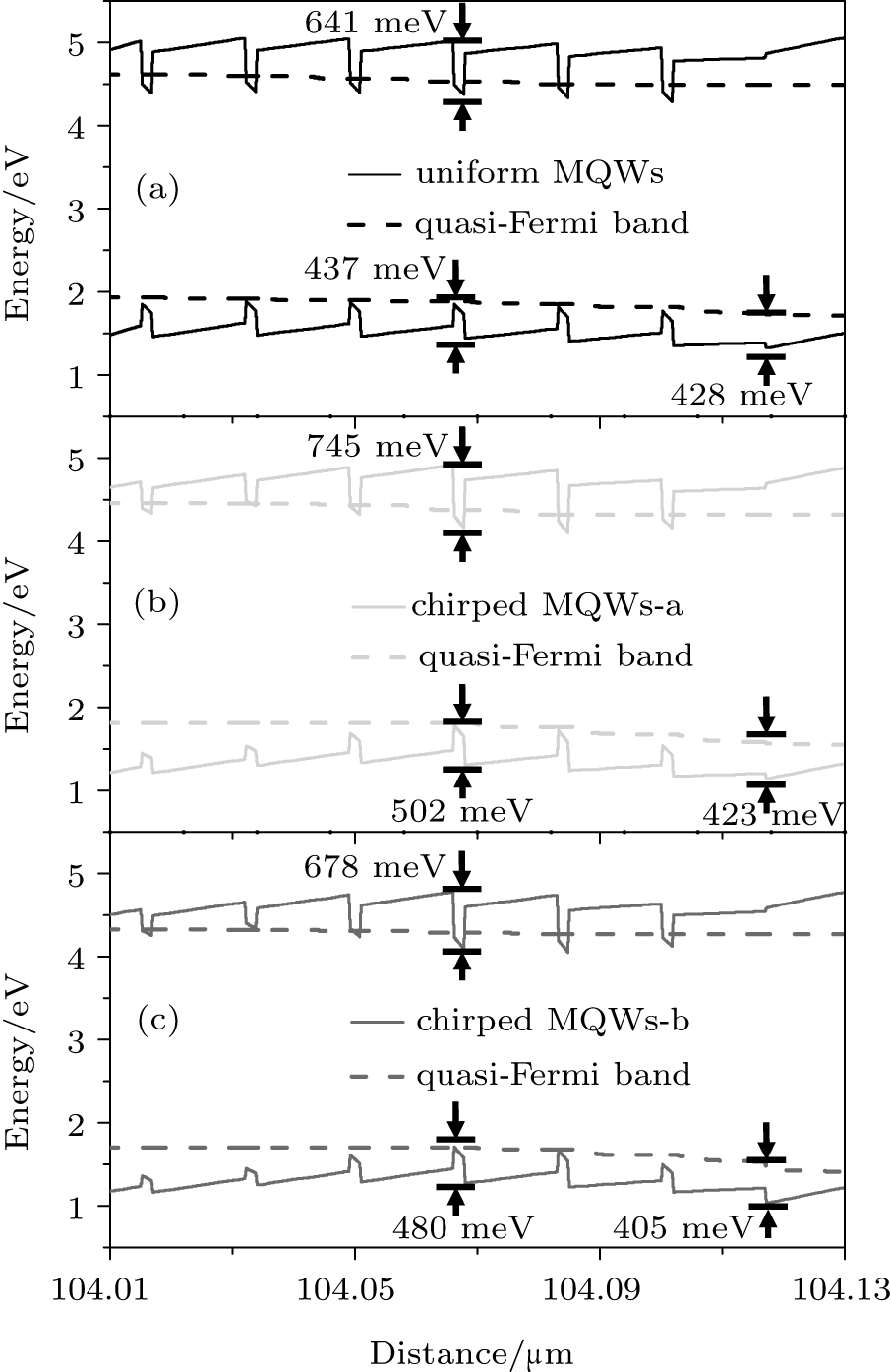
Figure 5 illustrates the energy-band diagrams near the active region of the uniform and chirped MQW structures at a 600 mA/mm2 injection current. The polarization field induced band bending, such as sloped triangular barriers and wells, deformed energy band of EBL and quasi-Fermi are calculated. According to the concept of energy band engineering, the band gap of the chirped QWs gradual decreases from n-side and p-side to the middle. It can be seen clearly in Fig. 5 that the fourth quantum well in the chirped MQWs-a structure is deeper than that in the uniform MQW structure (745 meV and 502 meV versus 641 meV and 437 meV for conduction and valence band, respectively), which can act as a reservoir to accumulate the electrons and holes.[17] Meanwhile, the fourth quantum well in chirped MQWs-b structure is deeper than that in the uniform MQW structure, but lower than that in the chirped MQWs-a structure (678 meV and 480 meV for conduction and valence band, respectively). In other words, the carriers in chirped MQW structures are more likely to inject into the fourth and fifth QWs for radiative recombination. Improved
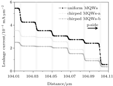
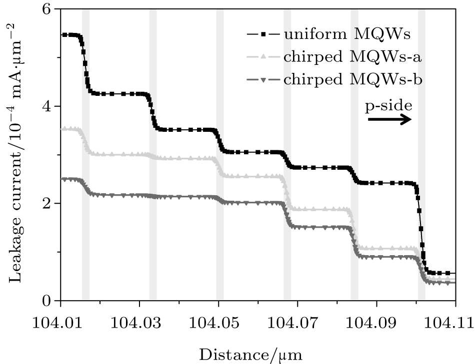
Fig. 6. Leakage current for LEDs with uniform and chirped MQW structures at 600 mA/mm2.
electron and hole injection efficiency of chirped MQW structure are significant reasons contributing to the suppression of efficiency droop. According to the results of chirped MQWs-b structure in Fig. 4, with the appropriate lower quantum barrier, further improvement of carrier injection efficiency can be achieved. Furthermore, holes play a more important role in radiative recombination than electrons as their injection efficiency is worse than electrons’ .[18] The effective potential height at the last-barrier/EBL interface in the valence band increases the difficulty for holes to transport into the active region, which results in poor hole injection efficiency.[5] Meanwhile, as electrons accumulated in the QWs close to EBL do not have enough holes to recombine, they are more likely to transport into the EBL and p-GaN layer by tunneling or thermo-electronic effect, resulting in a large leakage current. As illustrated in Fig. 5, the effective potential height for holes is reduced from 428 meV (uniform MQWs) to 423 meV (chirped MQWs-a), and 405 meV (chirped MQWs-b), respectively. As a result, compared to the uniform structure, the leakage currents of chirped structures are decreased significantly, while the injection current improved remarkably (shown in Fig. 6). In terms of chirped MQWs-b, the potential barriers declined slightly with the input of 2% doping of indium component in the middle five QBs. Meanwhile, the potential barrier declined and thus the reservoir effect of fourth and fifth QWs can get further enhancement. Therefore, compared with chirped MQWs-a, further suppression of the leakage current can be obtained (illustrated in Fig. 6).
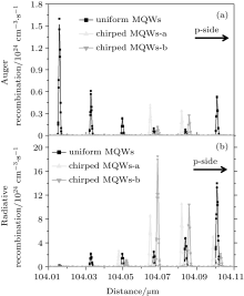
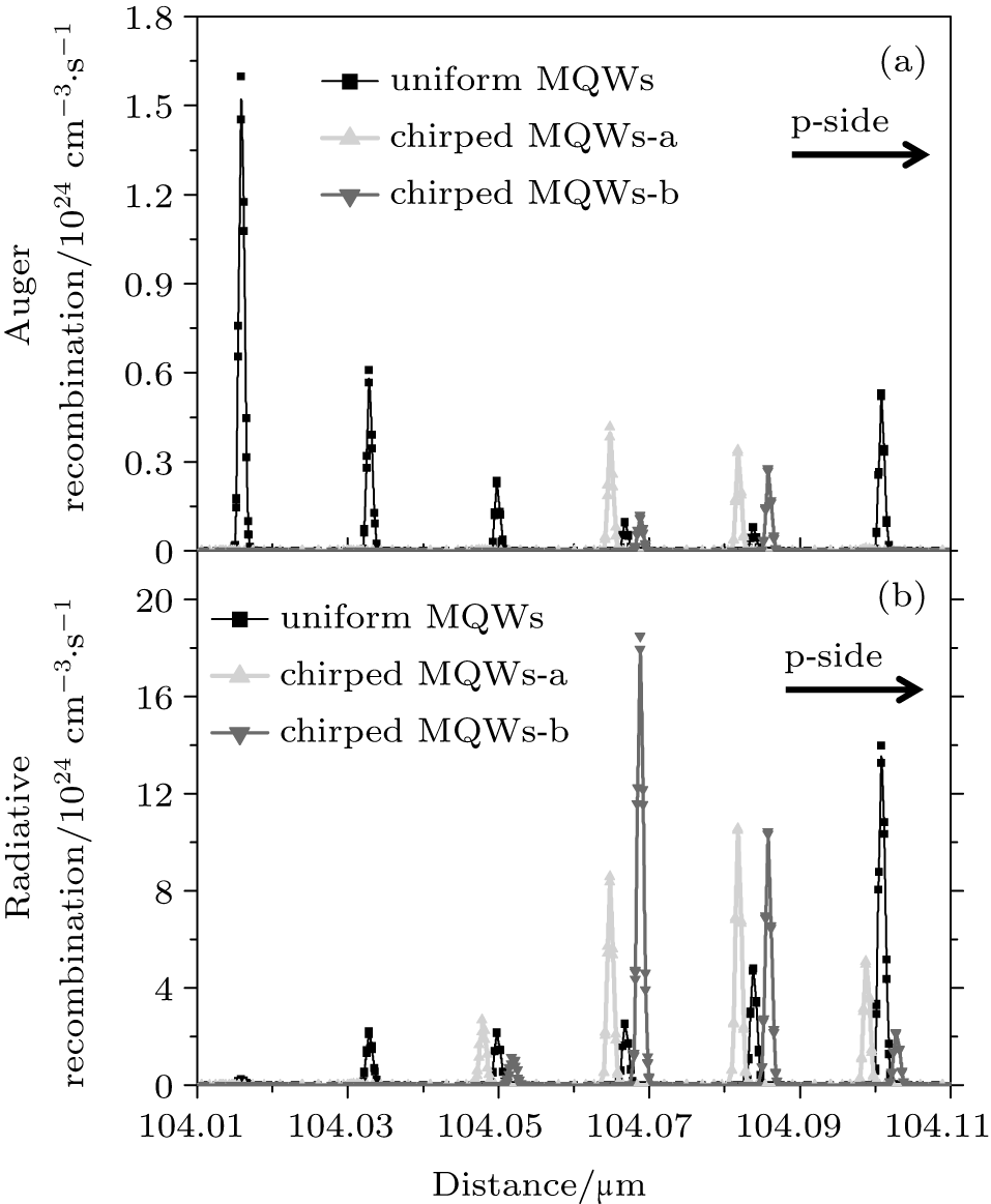
Figure 7 shows the Auger and radiative recombination rates of LEDs with uniform and chirped MQW structures at 600 mA/mm2. Due to the reservoir effect of the fourth and fifth QWs in chirped MQW structures, the radiative recombination rates are increased significantly, as the carriers have higher probability to be combined (illustrated in Fig. 7(b)). Furthermore, due to gradual changed component of indium in chirped MQW structures, the polarization effects could be decreased in the active region. As a result, the auger recombination rates of chirped MQWs are reduced, especially in the QWs close to the n-GaN layer (shown in Fig. 7(a)). The increase of auger recombination rate in the fifth QW of chirped MQWs may be ascribed to the significant augment of carriers. In the same carrier density, the auger recombination rates in chirped MQWs are lower than those in uniform MQWs. According to previous theoretical research, the Auger recombination is proposed as the root cause of the efficiency droop.[1, 4, 19] Therefore, the reduction of auger recombination in chirped MQW structures could make prodigious contributions to the efficiency droop suppression.
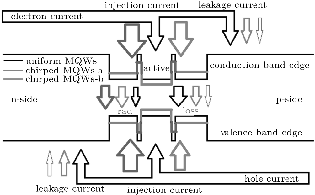
Figure 8 shows a schematic illustration of an energy band diagram for LED current components. The mechanism of chirped MQW structures is schematically illustrated in this figure. For the energy band diagram, the green line stands for the transformations from a uniform MQW structure to a chirped MQWs-a structure, while the red line stands for the transformations from chirped MQWs-a to chirped MQWs-b structure. As the results shown above, lower leaky current and Auger recombination can be obtained in the chirped MQW structure. In the meantime, the chirped MQW structures can also improve the injection current and radiative recombination, which contributes to the suppression of efficiency droop.
Fig. 8. Schematic illustration of energy band diagram for LED current components (rad– radiative recombination, loss– Auger recombination).
4. Conclusions
The results obtained experimentally and numerically indicate that GaN based LEDs can provide better optical performance and less efficiency droop when using the designed chirped MQW structures instead of the conventional uniform MQW structure. Compared to the conventional uniform LEDs, due to the improvement of carrier injection efficiency, LEDs with chirped MQW structures have lower turn on voltage and better IQE. The droop ratios of LEDs with chirped MQWs-a and MQWs-b structures show a remarkable improvement at 600 mA/mm2, reduced down from 28.6% (uniform LEDs) to 23.7% and 18.6%, respectively. Meanwhile, the maximum IQE increases from 76.9% (uniform LEDs) to 83.7% (chirped MQWs-a) and 88.6% (chirped MQWs-b). Moreover, compared with conventional uniform LEDs, the light optical power of LEDs with chirped MQW structures is enhanced by 15.1% and 27.4% at 600 mA/mm2 for chirped MQWs-a and chirped MQWs-b, respectively. The reservoir effect of chirped MQW structures may be the main reason as it could increase hole and electron injection efficiency and radiative recombination. As a result, a lower leakage current and Auger recombination rate of the chirped MQW structure can also be achieved. The chirped MQWs-b structure with lower potential barriers can enhance the reservoir effect and decrease the polarization effect. Therefore, compared with chirped MQWs-a structure, the chirped MQWs-b structure can obtain further improvement of the carrier injection efficiency and radiative recombination, as well as further efficiency of droop suppression. Related experiments are also on the way to verify the simulation results for chirped MQW structures.
ChenZ, YangW, LiuL, WanC H, LiL, HeY F, LN Y, WangL, LiD, ChenW H and HuX D2012Chin. Phys. B21108505DOI:10.1088/1674-1056/21/10/108505[Cited within:1][JCR: 1.148][CJCR: 1.2429]
12
ZakheimD A, PavluchenkoA S, BaumanD A, BulashevichK A, KhokhlevO V and KarpovS Y2012Phys. Status Solidi A209456DOI:10.1002/pssa.201100317[Cited within:1][JCR: 1.463]
LiX, OkurS, ZhangF, AvrutinV, ÖzgürÜ, MorkocH, HongS M, YenS H, HsuT C and MatulionisA2012J. Appl. Phys. 111063112DOI:10.1063/1.3699199[Cited within:1][JCR: 0.71]
16
ZhangL, DingK, LiuN X, WeiT B, JiX L, MaP, YanJ C, WangJ X, ZengY P and LiJ M2011Appl. Phys. Lett. 98101110DOI:10.1063/1.3565173[Cited within:1][JCR: 3.794]
17
DuC H, MaZ G, ZhouJ M, LuT P, JiangY, JiaH Q, LiuW M and ChenH2014Appl. Phys. Lett. 104151102DOI:10.1063/1.4871090[Cited within:1][JCR: 3.794]
18
RömerF and WitzigmannB2014Opt. Express22A1440DOI:10.1364/OE.22.0A1440[Cited within:1][JCR: 3.546]
19
Iveland J, MartinelliL, PerettiJ, SpeckJ S and WeisbuchC2013Phys. Rev. Lett. 110177406DOI:10.1103/PhysRevLett.110.177406[Cited within:1][JCR: 7.943]
2
2010
1.463
0.0
... [1] The efficiency droop phenomenon is observed across a broad wavelength spectrum, from blue and green InGaN/GaN LEDs to deep ultraviolet (UV) AlGaN/AlN LEDs ...
... [1,4,19] Therefore, the reduction of auger recombination in chirped MQW structures could make prodigious contributions to the efficiency droop suppression ...
1
2008
0.0
0.0
... [2,3] Auger recombination, defects, inefficient injection and transportation of holes as well as carrier overflow out of the active region have been identified to be significant reasons for efficiency droop ...
1
2010
3.794
0.0
... [2,3] Auger recombination, defects, inefficient injection and transportation of holes as well as carrier overflow out of the active region have been identified to be significant reasons for efficiency droop ...
2
2009
3.794
0.0
... [4#cod#x02013 ...
... [1,4,19] Therefore, the reduction of auger recombination in chirped MQW structures could make prodigious contributions to the efficiency droop suppression ...
1
2012
3.794
0.0
... [5] Meanwhile, as electrons accumulated in the QWs close to EBL do not have enough holes to recombine, they are more likely to transport into the EBL and p-GaN layer by tunneling or thermo-electronic effect, resulting in a large leakage current ...
1
2010
3.794
0.0
... 6] To reduce the efficiency droop of GaN-based LEDs, several research works have been performed by improvement of large V-shape pits, epitaxy, the electron-blocking layer (EBL) design and package design, etc ...
1
2014
0.71
0.0
... [7#cod#x02013 ...
1
2011
13.025
0.0
1
2013
1.463
0.0
... [9] In this work, the effective mass for mean free path calculation has been introduced into the mechanism of direct flying-over in transport models, which could make the carrier distribution results more accurate ...
1
2012
1.148
1.2429
1
2012
1.148
1.2429
... 11] Although significant steps forward have been made for the realization of high-brightness LEDs, it is still a big challenge to reduce the efficiency droop, especially at high injection current levels ...
1
2012
1.463
0.0
... As the hole and electron injection and transport in LEDs with conventional uniform MQWs have been found to be ineffective and non-uniform in the active region, which leads to dominant carrier localization in only one QW,[12] chirped MQW structures could be another way to improve carrier injection and suppress efficiency droop ...
1
2014
0.0
0.0
... [13] To improve the light output power (LOP), Chang et al ...
1
2012
3.385
0.0
... [14] However, based on their results, the efficiency droop effects become more serious ...
1
2012
0.71
0.0
... [15] In this work, we utilize two different chirped MQW structures to suppress efficiency droop and seek further promotion of hole-injection efficiency, as well as the improvement of LOP ...
1
2011
3.794
0.0
... [16] ...
1
2014
3.794
0.0
... [17] Meanwhile, the fourth quantum well in chirped MQWs-b structure is deeper than that in the uniform MQW structure, but lower than that in the chirped MQWs-a structure (678#cod#x00A0 ...
1
2014
3.546
0.0
... [18] The effective potential height at the last-barrier/EBL interface in the valence band increases the difficulty for holes to transport into the active region, which results in poor hole injection efficiency ...
1
2013
7.943
0.0
... [1,4,19] Therefore, the reduction of auger recombination in chirped MQW structures could make prodigious contributions to the efficiency droop suppression ...
Efficiency droop suppression in GaN-based light-emitting diodes by chirped multiple quantum well structure at high current injection*
[Zhao Yu-Kuna),b), Li Yu-Fenga),b), Huang Ya-Pinga),b), Wang Honga),b), Su Xi-Linc), Ding Wena),b), Yun Fenga),b),c)†]


 ]
]