†Corresponding author. E-mail: xuelinwang@sdu.edu.cn
*Project supported by the National Natural Science Foundation of China (Grant Nos. 11275117, U1432120, and 11274188) and the Heavy Ion Research Facility in Lanzhou (HIRFL), China.
We report the formation of two waveguide layers in a lithium niobate crystal by irradiation with swift heavy Kr ions with high (GeV) energies and ultralow fluences. The micro-Raman spectra are measured at different depths in the irradiated layer and show that the high electronic energy loss can cause lattice damage along the ion trajectory, while the nuclear energy loss causes damage at the end of the ion track. Two waveguide layers are formed by confinement with two barriers associated with decreases in the refractive index that are caused by electronic and nuclear energy losses, respectively.
Infrared light is the subject of considerable interest because it has broad applications in biomedical imaging, optical therapy, remote sensing, range finders, environmental monitoring, and fiber lasers, among other uses.[1– 3] Waveguide structures for infrared wavelengths have been studied in many materials, such as zinc selenide, [4] gallium lanthanum sulfide, [2] near-stoichiometric lithium niobate, [5] and zinc sulfide.[6] Lithium niobate (LiNbO3, LN) has a wide transmissive window in the spectral range from 400 nm in the visible range to approximately 5500 nm in the mid-infrared range, which provides an excellent platform for many applications in the infrared range. In addition, LN is an important material that is used in a wide range of photonic applications due to its intriguing electro– optical, acousto-optical, and nonlinear optical properties.[7] Many optical modulators, switches and amplifiers have been formed on LN waveguide structures. There are several techniques to form waveguide structures in LN crystals, such as ion implantation and proton exchange. Recently, swift heavy ion irradiation (energies greater than 1 MeV/amu) has emerged as a powerful method for waveguide fabrication in LN crystals.[5, 8] Compared with conventional ion (H, C, etc.) implantation, the fluences of swift heavy ions for waveguide fabrication are 4– 5 and 2– 3 orders of magnitude lower than the fluences of light ions (e.g., H, He) and heavier ions (e.g., C, O), respectively. The damage caused by the electronic energy loss of swift heavy ions dominates the damage caused by nuclear energy loss, which is different from the defects produced by conventional ion implantation.[8, 9] The damage caused by the electronic energy loss (Se) leads to a change in the refractive index and plays a significant role in the structural modification of the LN crystal. When the value of Se reaches a certain threshold, [10] partial or complete amorphous ion tracks can be generated in the material. Optical waveguide structures in the visible and near-infrared ranges in LN crystals and other materials have been produced using conventional ion implantation.[11] Very thick waveguides can be produced by swift heavy ion irradiation with ultralow fluences (< 1012 ion/cm2), and these devices may be useful for astrophysical applications in the mid-infrared range.[12, 13]
In this letter, we report the effect of two waveguide layers in LN crystals formed by swift heavy Kr ion irradiation with ultralow fluences, and we study the properties of these waveguide structures in the visible and mid-infrared ranges.
In this work, an x-cut LN sample is prepared from a wafer with dimensions of 6 mm × 3 mm × 1 mm. The surfaces of the wafer are optically polished, and then one of the surfaces is irradiated with swift Kr ions with an initial energy of 2.1 GeV at the Heavy Ion Research Facility in Lanzhou (HIRFL). A 70-μ m-thick Al foil is placed before the sample to slow down the incident Kr ions and reduce the ion energy to approximately 1.7 GeV. The incident Kr ion beam vertically irradiates the Al foil and the surface of the sample. The ion beam fluence is 1 × 10¹¹ ions/cm2.
Two terminal facets of the LN waveguide are polished carefully for end-face coupling experiments in the visible and mid-infrared ranges. Light from a 633-nm laser is coupled into the waveguide through a microscope objective lens. The light coupled out of the waveguide is then re-collimated with an objective lens, and an image is projected onto a screen or recorded by charge coupled device (CCD) cameras. A light with a 4-μ m wavelength from a tunable laser system– MIRTM 8025 is coupled into the irradiated layer through a MIR microscope objective lens. The light coupled out of the irradiated layer is collected by another MIR microscope objective lens and imaged onto a MIR CCD. The MIR microscope objective lens is composed of ZnSe with the following parameters: LFO-5-12-3.75 and N.A. = 0.13. The micro-Raman spectra of the swift-Kr-ion-irradiated LN crystal are measured using a micro-Raman spectrometer (Horiba/Jobin Yvon HR800), and a 633-nm beam with a 1-μ m spot size is focused on the polished end facet of the LN sample (as shown in Fig. 1(a)).
Figure 1(a) shows an optical micrograph of the polished end facet of the LN crystal; the irradiated layer can be seen clearly. The thickness of the irradiated layer is approximately 150 μ m. As we can see in Fig. 1(a), there are two dark lines: one line in the irradiated layer (marked L1) and the other line at the end of the ion track (marked L2) in the LN crystal.[14] As reported by Rivera, [13] two clearly distinct damage layers can be observed in an LN crystal when it is irradiated by ions with energies above 0.1 MeV/amu. The near-field intensity image of the light coupled out of the waveguide at 633 nm is recorded on the screen, as shown in Fig. 1(b). The propagation loss on samples ∼ 3-mm long is approximately 0.34 dB/cm, which is measured by the back-reflection method.[15] Combining with the value of the propagation loss in other work, [13, 16– 18] we can see that swift heavy ion irradiation is a competitive method for waveguide formation. In the end-face coupling experiments, the laser, the objective lens and the screen are kept motionless. A mask of opaque strip lines with a period of 200 μ m is used as a scale and placed on the stage instead of the LN sample to measure the thickness of the two light layers, as shown in Fig. 1(b). The total thickness of the two separated light layers is approximately 150 μ m. The TE-polarized fundamental guide mode of the thinner layer at the end of the ion track is recorded with the CCD camera, as shown in Fig. 1(c).
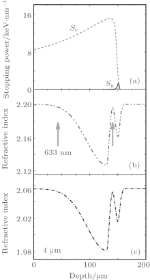
The electronic (Se) and nuclear (Sn) energy losses as functions of depth in a LN crystal are simulated using the Stopping and Range of Ions in Matter Code (SRIM 2010), [19] as shown in Fig. 2(a). The simulated ion range is consistent with the thickness (150 μ m) of the damaged layer shown in Fig. 1(a). From Fig. 2(a), we can see that Se is overwhelmingly dominant in the 0– 150 μ m range and has a peak value of 15.10 keV/nm at a depth of approximately 130 μ m, while Sn is very small near the surface and has a peak value of approximately 1.37 keV/nm at 150 μ m beneath the sample surface. The peak value of the electronic energy loss is high enough for damage formation and therefore leaves a damaged layer in the LN crystal corresponding to the “ L1” in Fig. 1(a).[20]
The amorphization caused by swift heavy ion irradiation induces a decrease in the refractive index in the LN crystal. It is assumed that the refractive index (ne) profile can be represented by four half-Gaussian curves. By adjusting the heights and the widths of the four half-Gaussian curves, the refractive index profile at 633 nm wavelength is obtained when the calculated mode profile agrees with the experimental one (Fig. 1(b)). The refractive index profile at 633 nm is shown in Fig. 2(b). The two waveguide layers indicated by arrows in Fig. 2(b) are confined by two barriers associated with the decrease in the refractive index that are formed by Se and Sn. These two waveguide layers correspond to the two light layers in Fig. 1(b). The thin waveguide layer at the end of the ion track forms a buried waveguide for 633-nm wavelength. The thicker layer can form a waveguide for much longer wavelengths, such as 4 μ m. The TE0 and TE1 mode profiles at a 4-μ m wavelength are recorded and shown in Figs. 3(a) and 3(b), respectively. As reported by Zelmon, [21] the Sellmeier equation for ne in LN crystal from 0.4 μ m to 5 μ m at 294 K is

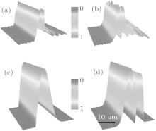
The refractive index ne at the wavelength of 4 μ m in LN crystal is calculated to be 2.0559. The refractive index profile at a 4-μ m wavelength is then estimated based on the refractive index (ne) profiles at 633 nm, as shown in Fig. 2(c). The commercial software “ BeamPROP” (BPM) is used to simulate light propagation in the waveguide. Figures 3(c) and 3(d) show the three-dimensional (3D) profiles of the TE0 and TE1 modes at a 4-μ m wavelength in the thick waveguide region calculated by BPM. There is good agreement between the simulated and measured mode profiles, which indicates that swift heavy ion irradiation is an effective method for the fabrication of waveguide structures at a wavelength of 4 μ m in the mid-infrared range.
 | Fig. 3. (a) The 3D near-field intensity profile of the TE modes at 4 μ m: (a) TE0 and (b) TE1 modes collected by CCD; (c) TE0 and (d) TE1 modes calculated by BPM. |
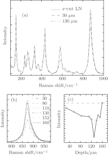
The Raman spectra at different depths in the Kr-ion-irradiated LN crystal and a virgin LN crystal are measured. For clarity, two Raman spectra in the irradiated layer and the Raman spectrum of the virgin LN crystal are shown in Fig. 4(a). The number and the positions of the Raman peaks are almost identical in all the spectra. The Raman intensities of all the peaks in the irradiated layer have the same trend with depth. The mode peak at 872 cm− 1A1 (LO) is intense; it is shown in Fig. 4(b) with numbers that indicate the depths at which the Raman spectra are obtained.[5, 17, 22] Figure 4(c) illustrates the variation of the intensities of the mode peak at 872 cm− 1 with depth. The two drops shown in Fig. 4(c) are consistent with the two barriers of the refractive index profile shown in Fig. 2(b) and are also consistent with the peaks of Se and Sn.
In conclusion, a waveguide structure is fabricated in an x-cut LN crystal using swift Kr ion irradiation with an energy of 1.7 GeV and a fluence of 1 × 10¹¹ ion/cm2. The near-field intensity profiles at the wavelengths of 633 nm and 4 μ m are obtained using end-face coupling setups. Two waveguide layers are formed by confinement by two barriers associated with the decreases in the refractive index caused by Se and Sn, respectively. Micro-Raman spectra at different depths in the irradiated layer are measured using a 633-nm laser source, and the two drops in the depth profile of the intensity of the Raman peak at 872 cm− 1 are consistent with the two barriers of the refractive index profile. These results demonstrate that swift heavy ion irradiation is a feasible method for fabricating waveguide structure in LN crystals in the mid-infrared range.
| 1 |
|
| 2 |
|
| 3 |
|
| 4 |
|
| 5 |
|
| 6 |
|
| 7 |
|
| 8 |
|
| 9 |
|
| 10 |
|
| 11 |
|
| 12 |
|
| 13 |
|
| 14 |
|
| 15 |
|
| 16 |
|
| 17 |
|
| 18 |
|
| 19 |
|
| 20 |
|
| 21 |
|
| 22 |
|


