Novel substrate trigger SCR-LDMOS stacking structure for high-voltage ESD protection application
[Ma Jin-Rong, Ming Qiao† , Zhang Bo]
, Zhang Bo]
|
|


†Corresponding author. E-mail: qiaoming@uestc.edu.cn
A novel substrate trigger semiconductor control rectifier-laterally diffused metal–oxide semiconductor (STSCR-LDMOS) stacked structure is proposed and simulated using the transimission line pulser (TLP) multiple-pulse simulation method in a 0.35-μm, 60-V biploar-CMOS-DMOS (BCD) process without additional masks. On account of a very low holding voltage, it is susceptible to latch-up-like danger for the semiconductor control rectifier-laterally diffused metal–oxide semiconductor (SCR-LDMOS) in high-voltage electro-static discharge (ESD) protection applications. Although the conventional stacking structure has achieved strong latch-up immunity by increasing holding voltage, excessive high trigger voltage does not meet requirements for an ESD protection device. The holding voltage of the proposed stacked structure is proportional to the stacking number, whereas the trigger voltage remains nearly the same. A high holding voltage of 30.6 V and trigger voltage of 75.4 V are achieved.
The popularity of the power integrated circuit (PIC) brings a lot of problems that need to be solved for electro-static discharge (ESD) protection in high-voltage circuits.[1– 4] To achieve a high breakdown voltage, the power device structure is implemented as an ESD device.[5] The conventional laterally diffused metal– oxide semiconductor (LDMOS) used as an output driver is always vulnerable to ESD.[6, 7] An effective method to solve this problem is to use a semiconductor control rectifier-laterally diffused metal oxide semiconductor (SCR-LDMOS); [8] however, its low holding voltage and latch-up immunity are challenging issues for its application.[9] Increasing the holding voltage is an effective way to achieve latch-up immunity of the ESD protection device.[10] Using a stacked device structure can achieve a high holding voltage. The simple stacked device structure, however, also brings an excessively high trigger voltage. A promising technique to reduce the trigger voltage is to use a substrate trigger silicon controlled rectifier (SCR).[11] The stacked substrate trigger SCR, which is triggered by an RC trigger circuit, [12] is only used for low-voltage ESD protection application.[13]
In this paper, a high holding voltage substrate trigger semiconductor control rectifier-laterally diffused metal– oxide semiconductor (STSCR-LDMOS) stacking structure is proposed and simulated in a 0.35-μ m, 60-V biploar-CMOS-DMOS (BCD) process. The holding voltage can be increased by increasing the stacked number of the cells whereas the trigger voltage keeps as low as that of one single cell. A high holding voltage of 30.6 V with a low trigger voltage of 75.4 V can be simultaneously achieved without an additional process and mask.
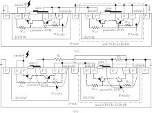
A conventional stacked SCR-LDMOS structure and the proposed stacked STSCR- LDMOS structure are respectively shown in Figs. 1(a) and 1(b), and the unit-SCR-LDMOS and unit-STSCR-LDMOS are respectively shown in the two dashed boxes in Figs. 1(a) and 1(b). The unit-SCR-LDMOS includes two parasitic transistors P2 and N2, which comprises a parasitic SCR. Compared with the unit-SCR-LDMOS structure, the unit-STSCR-LDMOS structure is added with a p-type heavy doping region in the p-body, as a p-trig terminal. The operating principle of the unit-STSCR-LDMOS structure is as follows. When current is injected from the p-trig terminal, the voltage on the resistance Rp2 will trigger parasitic transistor N2, and the current of N2 will flow through the resistance Rn2, which will trigger parasitic transistor P2. Finally, N2 and P2 form positive feedback, that is, parasitic SCR is triggered. In addition, adding the p-trigger electrode increases the size of the p-body and base width of parasitic transistor N2, which will reduce the magnification β of parasitic transistor N2 and weaken the effect of positive feedback between transistors N2 and P2. Therefore, the holding voltage of the unit-STSCR-LDMOS is higher than that of the unit-SCR-LDMOS. A comparison of the holding voltage is listed in Table 1.
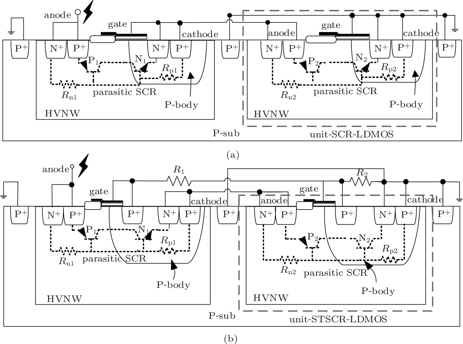 | Fig. 1. Schematic cross-sectional views of (a) the conventional SCR-LDMOS stacking structure and (b) the proposed STSCR-LDMOS stacking structure. |
| Table 1. Comparison of holding voltage. |
The conventional SCR-LDMOS stacking structure is the direct stacking of the unit-SCR-LDMOSs, while the proposed STSCR-LDMOS stacking structure is not only the stacking of the unit-STSCR-LDMOS, but also connected with the resistance which is used to trigger the stacking structure. As shown in Fig. 1(b), the trigger resistance R1 connects with two p-trig terminals, the trigger resistance R2, and two gates. A high voltage N-well isolates the unit-STSCR-LDMOS from the others, so the proposed stacking structure does not require an additional process nor a mask. In order to improve the holding voltage, more than two stages of stacked STSCR-LDMOS may be required in practical applications.
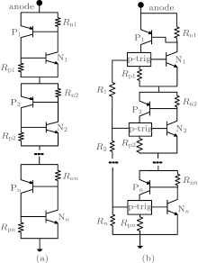
The equivalent circuits of the conventional and proposed stacking structure are shown in Figs. 2(a) and 2(b). Under ESD stress, each SCR-LDMOS needs to be triggered by breakdown for the conventional SCR-LDMOS stacking structure, so the trigger voltage of which is the sum of that of each SCR-LDMOS. For the proposed STSCR-LDMOS stacking structure, except for the first unit-STSCR-LDMOS, the trigger voltages of the others are all very small because their trigger modes each are the current injection from the p-trig terminal, rather than the breakdown of the internal junction. Parasitic transistor P1 which has been triggered will provide the trigger current for other STSCR-LDMOSs by the trigger resistances R1, R2, and Rn. Then each STSCR-LDMOS will be triggered and discharge the ESD current. Therefore, the trigger voltage of the proposed STSCR-LDMOS stacking structure depends mainly on the breakdown voltage of parasitic transistor P1, that is, the trigger voltage of the first STSCR-LDMOS. In addition, the holding voltage of the proposed stacking structure is the sum of that of each unit cell. In normal operation, the stacking structure is in the off-state, and will not affect the normal work of the internal circuit because the working voltage is less than the trigger voltage of STSCR-LDMOS.
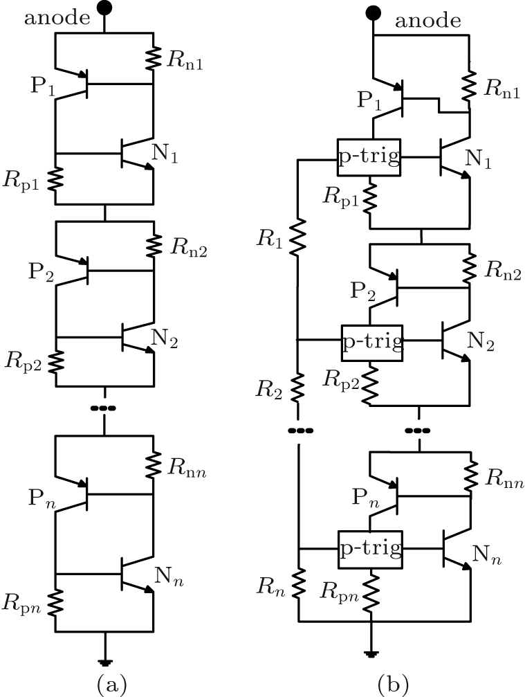 | Fig. 2. Equivalent circuits for (a) conventional SCR-LDMOS stacking structure and (b) proposed STSCR-LDMOS stacking structure. |
The simulation model of the ESD protection device has attracted extensive attention.[14– 16] To analyze the performance of the proposed stacking structure, a novel simulation method, TLP multiple-pulse simulation is used by Ding et al.[17] Because of the many advantages of this method, it is necessary to introduce the simulation method here.
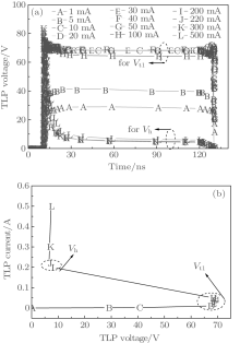
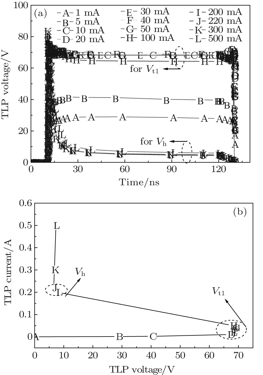
This method is similar to the actual TLP test. A series of current pulses with increasing amplitude, 10 ns of rise time, 100 ns of duration time, is applied to both ends of the simulation device. Then a series of voltage pulses will be obtained by the transient simulation of each current pulse. Figure 3(a) shows the voltage pulse of the conventional SCR-LDMOS, where the curves of the voltage pulse are marked with different letters. Each current pulse and the average of 70%∼ 90% of the corresponding voltage will constitute a point of the TLP I– V curve, by linking the series of points into a line, thereby obtaining a TLP I– V curve. Figure 3(b) shows the TLP I– V curve extracted from Fig. 3(a). Each point is marked with a letter which corresponds to the letter of Fig. 3(a). The device parameters are listed in Table 2.
 | Fig. 3. (a) A series of voltage responses obtained by the transient simulation; (b) simulated TLP I– V curve. |
| Table 2. Device parameters used in the simulation. |
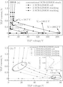
Figure 4(a) shows the simulated TLP I– V curves of the conventional stacked SCR-LDMOS structure with the stacking number increasing from 1 to 3 by using the method of TLP multiple-pulse simulation. The trigger voltage increases from 70.7 V to 208.2 V and the holding voltage increases from 6.4 V to 18.7 V. The holding voltage increasing with the stacking number is consistent with our expected result. However, the trigger voltage is also proportional to the stacking number, which is undesired for HV ESD.
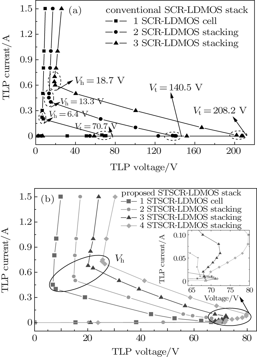 | Fig. 4. Simulated TLP I– V characteristics of (a) the conventional SCR- LDMOS stacking structure, (b) the proposed STSCR-LDMOS stacking structure with R1 = R2 = Rn = 100 Ω . |
Figure 4(b) shows the simulated TLP I– V curve of the proposed stacked STSCR-LDMOS structure with the stacking number increasing from 1 to 4, and trigger resistance being 100 Ω . There are twice the snapback phenomena. At the first time the parasitic transistor P1 is triggered, the breakdown voltage increases only from 70.2 V to 71.6 V when the stacking number increases from 1 to 4. At the second time the transistor P1 provides an adequate trigger current for the stacked STSCR-LDMOS structure, all of the parasitic SCRs will be triggered, and the trigger voltage of the second snapback increases from 66.7 V to 79.7 V when the stacking number increases from 2 to 4. Therefore, the trigger voltage of the STSCR-LDMOS stacking structure increases from 70.2 V to 79.7 V and the holding voltage increases from 6.9 V to 25.4 V when the stacking number increases from 1 to 4.
Therefore, the novel STSCR-LDMOS stacking structure has a high holding voltage which is the sum of that of the unit cell and a low trigger voltage, which depends mainly on the trigger voltage of the first STSCR-LDMOS. A high holding voltage ensures that the novel STSCR-LDMOS stacking structure has strong latch-up immunity. A low trigger voltage ensures that the stacking structure can be triggered quickly under ESD stress. Therefore, the proposed stacked STSCR-LDMOS structure is attractive to high-voltage ESD protection applications. Increasing the magnification β of parasitic transistor P1 can reduce the holding voltage of transistor P1, and reduce the second snapback trigger voltage of the stacking structure, which may reduce the trigger voltage of the stacking structure. The second snapback trigger current increases from 10 mA to 100 mA when the stacking number increases from 2 to 4, which is also conducible to noise immunity.
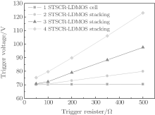
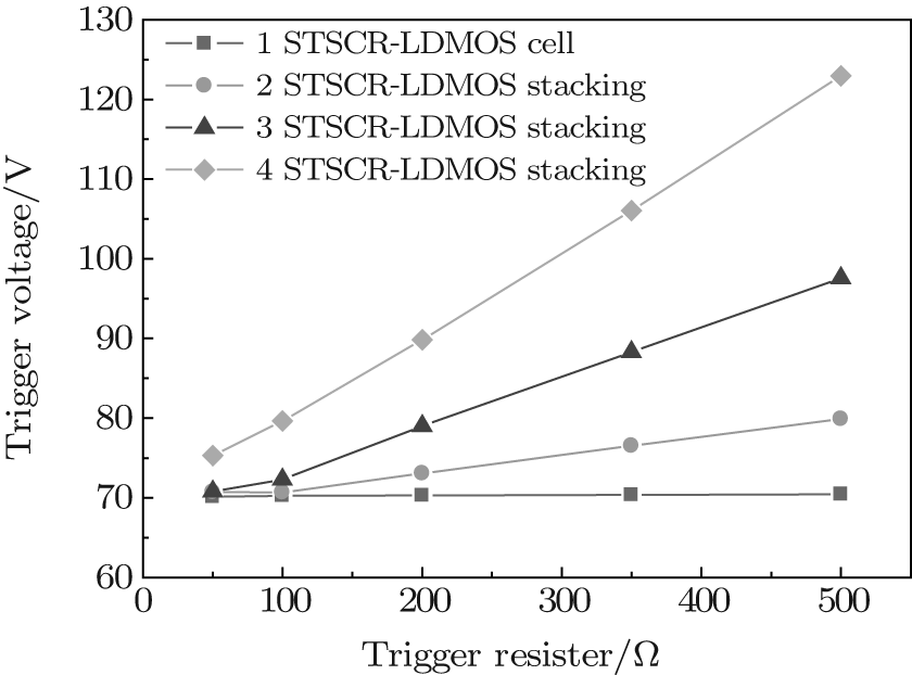
Trigger resistances R1, R2, and Rn have an important influence on the trigger voltage of the proposed stacked STSCR-LDMOS structure. Figure 5 shows the trigger voltage characteristics of the proposed STSCR-LDMOS stacking structure. The greater the trigger resistance, the faster the trigger voltage increases with the stacking number, because the big trigger resistance will result in the trigger voltage of the second snapback increasing quickly, as shown in Fig. 4(b). The trigger voltage increases from 70.1 V to 75.36 V when the trigger resistance is 50 Ω . However, the trigger voltage increases from 70.43 V to 122.95 V when the trigger resistance is 500 Ω . In addition, the trigger resistance has little influence on the trigger voltage for one STSCR-LDMOS. The trigger voltage, however, will increase with increasing the trigger resistance and the stacking number for two or more STSCR-LDMOS.
 | Fig. 5. Trigger voltage characteristics of the proposed STSCR-LDMOS stacking structure. |
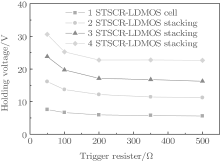
Trigger resistances R1, R2, and Rn also have an important influence on the holding voltage of the proposed stacking structure. Figure 6 shows the holding voltage characteristics of the proposed STSCR-LDMOS stacking structure. The holding voltage increase is proportional to the stacking number, for example, it increases from 7.57 V to 30.6 V when the trigger resistance is 50 Ω . The holding voltage remains nearly the same when the trigger resistance is greater than 200 Ω . However, it increases with reducing the trigger resistance when resistance is less than 200 Ω . The reason is that the current flowing from the p-trig terminal of the first STSCR-LDMOS, after the stacking structure has been triggered, increases gradually with reducing the trigger resistance.
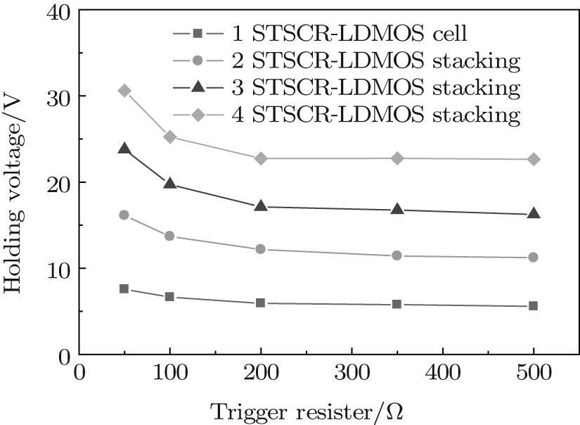 | Fig. 6. Holding voltage characteristics of the proposed STSCR-LDMOS stacking structure. |
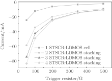
Figure 7 shows the current characteristics of the p-trig terminal of the first STSCR-LDMOS when the TLP current pulse is 800 mA. The increasing of the current of the p-trig terminal means that the base current of N1 will decrease, which leads to the decrease of the collector current of N1. Therefore, the effect of positive feedback between P1 and N1 is weakened, which results in the decrease of the magnification of the parasitic SCR. Finally, the holding voltage of the first STSCR-LDMOS will increase, that is, the holding voltage of the proposed stacking structure increases.
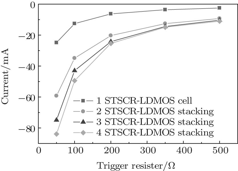 | Fig. 7. Current characteristics of the p-trig terminal of the first STSCR-LDMOS. |
According to the above analysis, trigger resistances R1, R2, and Rn have an important influence on the trigger voltage and holding voltage of the proposed stacked STSCR-LDMOS structure. The selection of resistance will determine the performance of the stacking structure. When the resistance is greater than 200 Ω , the excessively high trigger voltage cannot meet the requirements for the ESD protection device. When the resistance is less than 50 Ω , although the holding voltage of the proposed stacking structure increases, the current from the p-trig terminal of the first STSCR-LDMOS increases rapidly, which may produce a large amount of heat in the place where the breakdown of the first STSCR-LDMOS takes place, causing the failure current to decrease. Therefore, the best choice of the resistance should be in the range from 50 Ω to 200 Ω .
A novel stacked STSCR-LDMOS structure is proposed and simulated in a 0.35-μ m, 60-V BCD process. The holding voltage can be adjusted by the number of stacking units, whereas the trigger voltage is determined mainly by the first STSCR-LDMOS. In this paper we discuss and prove that the best trigger resistance is in the range from 50 Ω to 200 Ω . A holding voltage of 30.6 V and a trigger voltage of 75.4 V are both achieved when the trigger resistance is 50 Ω . The high holding voltage and low trigger voltage of the proposed STSCR-LDMOS stacking structure make it very fascinating for high voltage ESD protection.
| 1 |
|
| 2 |
|
| 3 |
|
| 4 |
|
| 5 |
|
| 6 |
|
| 7 |
|
| 8 |
|
| 9 |
|
| 10 |
|
| 11 |
|
| 12 |
|
| 13 |
|
| 14 |
|
| 15 |
|
| 16 |
|
| 17 |
|