†Corresponding author. E-mail: hqin2007@sinano.ac.cn
*Project supported by the National Natural Science Foundation of China (Grant Nos. 61271157, 61401456, and 11403084), Jiangsu Provincial Planned Projects for Postdoctoral Research Funds (Grant No. 1301054B), the Fund from Suzhou Industry Technology Bureau (Grant No. ZXG2012024), China Postdoctoral Science Foundation (Grant No. 2014M551678), the Graduate Student Innovation Program for Universities of Jiangsu Province (Grant No. CXLX12_0724), the Fundamental Research Funds for the Central Universities (Grant No. JUDCF 12032), and the Fund from National University of Defense Technology (Grant No. JC13-02-14).
We report the fabrication and characterization of a single-layer graphene field-effect terahertz detector, which is coupled with dipole-like antennas based on the self-mixing detector model. The graphene is grown by chemical vapor deposition and then transferred onto an SiO2/Si substrate. We demonstrate room-temperature detection at 237 GHz. The detector could offer a voltage responsivity of 0.1 V/W and a noise equivalent power of 207 nW/Hz1/2. Our modeling indicates that the observed photovoltage in the p-type gated channel can be well fit by the self-mixing theory. A different photoresponse other than self-mixing may apply for the n-type gated channel.
Sensitive terahertz detection is of great importance to a variety of potential applications, such as communication, [1] medicine development, [2] and security checking.[3] Field-effect transistors (FETs) based on high-electron-mobility two-dimensional electron gas (2DEG) have been proved to be such detectors suitable for room-temperature applications.[4, 5] Graphene has attracted great attention due to its distinctive physical properties, such as zero band gap and high carrier mobility.[6] FETs based on graphene produced by mechanical exfoliation has been recently demonstrated for terahertz detection at 300 GHz.[7] The exfoliated graphene films, however, are limited to hundreds of squared micrometers, thus are not scalable to meet a wide range of applications.[8] The large, flexible, and transferable graphene films synthesized with a simple and scalable method can enable practical applications. Chemical vapor deposition (CVD) has emerged as an important method to produce graphene since first reported in 2008.[9] Here we report the fabrication and characterization of an FET terahertz detector based on graphene grown by CVD. Detailed device parameters such as the carrier mobility, the derivative of conductance, and the series resistance are extracted. By using the self-mixing model, we evaluate the terahertz response and compare it to our experimental values.
The device designed for evaluating the terahertz self-mixing in graphene field-effect transistors (GFET) is the same as that reported in Ref. [10]. The schematic cross section and the equivalent circuit of the detector are shown in Fig. 1(a). A single-layer graphene (SLG) grown by CVD on Cu was transferred onto a p-type (1 × 10− 3 Ω · cm– 5 × 10− 3 Ω · cm) Si substrate (550 µ m) covered with SiO2 (285 nm) via the PMMA-mediated approach.[11] Prior to the fabrication, the quality of graphene is examined by Raman spectroscopy with a 514-nm laser (Fig. 1(b)). The large intensity ratio of 2D band (2680 cm− 1) over G band (1580 cm− 1) clearly confirms the existence of SLG.[12] Ultra-violet (UV) lithography followed by oxygen plasma etching was used to define the channel. The source and drain electrodes were introduced by a standard sequence of UV lithography, evaporation of Ti/Au (20 nm/180 nm) and lift-off. To achieve a uniform ultrathin gate dielectric layer, perylene tetracarboxylic acid (PTCA) was used to functionalize the SLG with densely packed functional groups.[13] Then a 19-nm Al2O3 layer was deposited on graphene by atomic layer deposition (ALD) at 150 ° C as the gate insulator with a dielectric constant of 7.5. The top gate and the antennas were realized by using the same evaporation and lift-off processes as for the source and drain electrodes. The leakage current density through the top-gate dielectric is lower than 8 pA/µ m2 at an electric field strength of − 3 × 10⁶ V/cm∼ + 6 × 10⁶ V/cm. The gate-leakage current is small compared with the THz-induced current and the dc drain– source current, indicating that the gate leakage current can be neglected in the terahertz detection.
The top-view of the GFET detector is shown in Fig. 1(c). The core-active graphene channel is under the central gate. The antennas are designed to enhance the local terahertz field under the gate upon the incident terahertz radiation. The top-gate length (L) is 2 µ m and the gated channel width (W) is 5 µ m. Each antenna block is 90 µ m × 10 µ m in size. The two i-antennas are isolated from the top-gate and the Ohmic contacts. The gap between the gate and each i-antenna is 2 µ m. The Ohmic contacts are about 26 µ m from the isolated i-antennas.
Upon terahertz irradiation, a DC self-mixing photocurrent is generated in the SLG channel under the top gate. When the source– drain voltage is zero, the effective gate voltage is constant throughout the gated SLG channel. The self-mixing photocurrent can be written as[14]

where G0 is the gated SLG channel conductance, VTG is the voltage on the top gate, Z0 = 367.7 Ω is the free-space impedance, P0 is the energy flux of the terahertz irradiation, and 
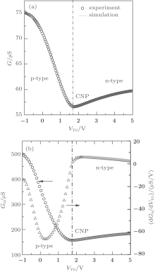
Figure 2(a) shows the top-gated conductance of the GFET, exhibiting clear ambipolar characteristics. The charge neutrality point (CNP) is located at positive VTG (1.75 V), indicating that the graphene is of p-type. The width of the top gate electrode is much smaller than the source– drain distance. When VTG > VCNP, the top-gated channel and ungated regions is n type and p type, respectively. The resistance of the p– n junction will increase with VTG, which is attributed to the apparent asymmetry between electron and hole conductances.[15] In order to gain quantitative insight into the extracted conductance of the gated SLG channel and avoid the effect of p– n junction, we adopt the model reported in Ref. [16] to analyze the hole conductance of the GFET. The hole density in the graphene channel can be approximated by 


where μ is the carrier mobility and α = L/W = 0.4 is the ratio of length to width of the graphene channel tuned by the gate. RT is the series resistance which includes both the Ohmic contact resistances and the resistance from the ungated graphene. The fit agrees well with the experimental data, as shown in Fig. 2(a). The extracted parameters are summarized in Table 1, and the gated SLG channel conductance (G0 = 1/R0 = 1/(R− RT)) is shown in Fig. 2(b).
 | Fig. 2. (a) The measured (circles) and fit (curve) source– drain conductances as a function of VTG. (b) The extracted conductance of the gated SLG channel (circles) and its derivative (triangle). |
| Table 1. Extracted parameters of the GFET at room temperature. |
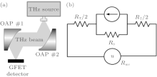
Both the experimental setup for THz radiation detection and the equivalent circuit of the detector in the photovoltage mode are shown in Fig. 3. The radiation at 237 GHz from a Virginia Diodes Inc (VDI) source (Model Number: Tx-165) with a power of Pt = 3 mW is chopped at 1 kHz and focused onto the GFET detector by a set of two off-axis parabolic (OAP) mirrors. The photovoltage between the drain and the source is measured by means of a lock-in amplifier (SR830) following a voltage preamplifier (SR560). The output photovoltage can be written as

where Rmv = 1 MΩ is the input impedance of the voltage preamplifier.
 | Fig. 3. (a) The experiment setup for THz detection. (b) The equivalent circuit of the GFET detector. |
Since the effective area of our detector is slightly smaller than the diffraction-limited area Sλ = λ 2/4, the voltage responsivity is approximated as[17]

Given our beam diameter d = 4 mm, the radiation beam spot area (St = π d2/4) is 12.6 mm2. As shown in Fig. 4(a), the experimental voltage responsivity and simulated voltage responsivity as a function of VTG vary from negative to positive, consistent with the ambipolar nature of transport in graphene. The maximum experimental voltage responsivity is 0.1 V/W with VTG = 3.83 V when the gated channel is n-type. The experimental values are in excellent agreement with the fitting curve predicted by the self-mixing model in the region of VTG < VCNP. However, the fitting values of Rv are apparently smaller in the region of VTG > VCNP. Owing to the presence of the p– n junction between the top-gated region and ungated regions, the photovoltage has become more complicated. The effect of the p– n junction is not included yet in our model which may contribute to the observed optoelectronic response when the gated channel is tuned into n-type.[18]
 | Fig. 4. (a) The measured and the simulated terahertz response as a function of VTG. (b) The measured and calcalated thermal-noise limited NEP of the detector at room temperature. |
Apart from the responsivity, the relevant figure of merit to characterize a photodetector is the NEP. The noise levels of the lock-in amplifier and the voltage preamplifier are less than 6 nV/Hz1/2 and 4 nV/Hz1/2, respectively. Thus the noise from the experimental setup can be neglected. The noise level of the GFET detectors is dominated by thermal noise when no source– drain voltage is applied. The NEP limited by the thermal noise can be expressed as

where kB is the Boltzmann constant and T = 300 K is the room temperature.[19] The experimental NEP of the detector as a function of VTG was measured at 1 kHz with a bandwidth of 1.25 Hz. As shown in Fig. 4(b), the minimum experimental NEP is 207 nW/Hz1/2 when the gated channel is n-type, which is very close to the thermal-noise limited NEP at room temperature. The minimum experimental NEP in the n-type gated channel is lower than that in the p-type gated channel, which maybe the effect of a different photoresponse other than self-mixing. For optimum NEP, a lower noise floor is required. To achieve an even lower thermal-noise limited NEP, it requires the RT to be sufficiently low. So there is still room to improve the NEP by improving the material quality and the fabrication technology.
In summary, we have fabricated an FET terahertz detector based on graphene grown by CVD. At room temperature, the voltage responsivity of the detector is 0.1 V/W and the NEP is 207 nW/Hz1/2 at 237 GHz. Our self-mixing model well describes the main features of the terahertz response. Further advances are expected by understanding and exploiting the new physics of the p– n junction, which may optimize THz detectors with even lower NEP.
| 1 |
|
| 2 |
|
| 3 |
|
| 4 |
|
| 5 |
|
| 6 |
|
| 7 |
|
| 8 |
|
| 9 |
|
| 10 |
|
| 11 |
|
| 12 |
|
| 13 |
|
| 14 |
|
| 15 |
|
| 16 |
|
| 17 |
|
| 18 |
|
| 19 |
|


