†Corresponding author. E-mail: sjx@uestc.edu.cn
*Project supported by the National Natural Science Foundation of China (Grant No. 31470822).
The mobility edge (ME) model with single Gaussian density of states (DOS) is simplified based on the recent experimental results about the Einstein relationship. The free holes are treated as being non-degenerate, and the trapped holes are dealt with as being degenerate. This enables the integral for the trapped holes to be easily realized in a program. The J– V curves are obtained through solving drift-diffusion equations. When this model is applied to four organic diodes, an obvious deviation between theoretical curves and experimental data is observed. In order to solve this problem, a new DOS with exponential tail is proposed. The results show that the consistence between J– V curves and experimental data based on a new DOS is far better than that based on the Gaussian DOS. The variation of extracted mobility with temperature can be well described by the Arrhenius relationship.
In spite of the recent progress made in organic electronic thin-film devices both in theoretical and experimental aspects, the physical mechanism of charge transport has not been thoroughly determined. The popular models reported in the literature can be divided into two types. The first type is the hopping model. It usually combines with kinetic Monte Carlo simulations, the concept of a transport level, effective-medium theory, [1– 4] or percolation theory.[5– 9] The second type of model is the mobility edge (ME) model[10– 17] firstly proposed by Mott.[10, 11]
In the ME model, [10– 17] the electronic states are divided into two non-overlapping state distributions, one is corresponding to the localized (trap) states and the other to the delocalized (band) states; the two distributions are separated by an energy level referred to as the ME. An additional assumption frequently made within the ME model is that, in contrast to the hopping model, the charge carriers in the localized states are completely immobile; thus, only the carriers that are thermally activated into the band states contribute to charge transport. Dacuna et al., [15] and Dacuma and Salleo[16] applied the ME model with single Gaussian density of states (DOS) to an organic diode with rubrene single crystal, and they obtained very good results for current– voltage (J– V) curves at different temperatures as compared with experimental data. However, they[15, 16] show that the ME model with non-Gaussian DOS cannot arrive at good agreement with experimental data.
Recently, Mehraeen et al.[17] provided a detailed comparison of the hopping model with the ME model in describing the effects of charge– carrier concentration on electrical conductivity, carrier mobility, and position of the Fermi level in the case of such a composite DOS. Their results from the two models show similar trends.[17] They also used both models to explain the recent experimental data reported on n-doped C60 films. Their results indicate that both models can reproduce very well the experimental dependences of electrical conductivity, carrier mobility, and Fermi energy on charge concentration.
Although the ME model with Gaussian DOS has been shown successfully at present, [15– 17] we notice that the types of materials the ME model have been applied to are fairly limited. Only one diode with rubrene single crystal has been studied in the respect of the J– V property.[16] In order to check the reasonability and applicability of the ME model, it is necessary to apply the model to more materials. In this paper, we present the modified version of the ME model, and apply it to four diodes comprised of different materials.
Although the Gaussian DOS is popular for organic semiconductors, recently some authors[18– 23] emphasized the importance of DOS. Some authors proposed that the DOS should have an exponential tail, and some authors suggested different forms of DOS. Puigdollers et al.[18] calculated the DOSs in the gap of pentacene from the electrical characteristics of thin-film transistors, measured at different temperatures. They confirmed the existence of the exponential tail. Kalb and Batlogg[19] calculated the trap DOSs in organic field-effect transistors from experiment and compare the results from different methods and results for thin-film transistors and single crystals. Oelerich et al.[20] proposed the trial DOS function N0 exp [− (E − Ev)λ /σ λ ] and found only those with λ > 1.8 can explain the experimental results of mobility. Yogev et al.[21] directly measured DOSs in pentacene thin film transistors. Cho et al.[22] studied the trap DOSs in n-channel organic transistors, Welborn et al.[23] studied the DOSs for disordered systems from free probability.
Most of the above authors[18– 23] proposed a combination of Gaussian DOS with an additional exponential term, i.e., N0 exp[(E − Ev)/σ ] (E < Ev). However, such a combination adds two more parameters, and exponential term N0 exp[(E − Ev)/σ ] is divergent as E tends to infinity, which is unreasonable, and it should be cut short artificially. In view of this analysis, it is needed to develop a new DOS with an exponential tail such that the shortcoming of the above combination can be eliminated, by which we are motivated to proposing a new DOS with an exponential tail in this paper.
The Gaussian and new DOSs, each with width σ , and central energy level Ev used in the ME model, are respectively

and

Both DOSs satisfy the normalizing condition, ∫ D(E) dE = N0. It can be seen that each of the new DOSs indeed has an exponential tail and is always convergent as E → ± ∞ . Near the center of the DOS, (E − Ev) → 0, equations (1) and (2) can be expanded into the following form respectively

and

Thus each of the new DOSs has a varying tendency similar to the one that the Gaussian DOS has near the center of the DOS.
The densities of free and trapped holes in terms of single Gaussian DOS can be expressed as

and

where


Em is the ME, electronic states with energies higher than ME are localized (trap) states, and the other are delocalized (band) states. The f(E) is the Fermi– Dirac (FD) distribution function for holes, EF is the Fermi energy level without external electric field, and EF (x) = EF + qφ (x) is the quisi-Fermi energy level. There is no constant EF (x) in a device under space charge-limited (SCL) conditions, but the separated EF should be a constant. Equations (5)– (7) are fundamental formulas for the ME model.
Some studies[24– 28] pointed out that the Fermi– Dirac statistics used in Eqs. (5) and (6) would lead to a generalized Einstein relation (GER), D/μ = − pf [qdpf/dEF]− 1, instead of the traditional one, D/μ = kT/q, where D is the diffusion coefficient of holes and μ is the mobility. However, Neumann et al.[29] did not support the GER through theoretical analysis. Wetzelaer et al.[30] confirmed the validity of the Einstein relation in organic semiconductors by studying the diffusion-driven currents of single-carrier diodes. As is well known, in inorganic semiconductor physics, the traditional Einstein relation is related to the non-degenerate Boltzmann statistics.
It should be pointed out that although the same FD distribution f(E) is used in both Eqs. (5) and (6), the results of Refs. [29] and [30] show that the traditional Einstein relationship is valid for organic semiconductors, this implies that the organic semiconductors should be non-degenerate, (EF − Ev) ≫ kT. So even under the SCL conditions, the quasi-Fermi energy EF(x) also satisfies the non-degenerate condition, (EF − Ev) ≫ kT. This means that the free holes can be seen as being non-degenerate, and the trapped holes should be treated as being degenerate. When the Fermi– Dirac distribution in Eq. (7) is applied to free holes and trapped holes, it can and cannot be approximated by Boltzmann distribution, respectively. Equation (5) for free holes can be approximated by the following form

Introducing the effective DOS

the density of free holes can be expressed as

Although the Fermi– Dirac distribution in Eq. (7) cannot be approximated by Boltzmann distribution when applied to trapped holes in Eq. (6), we can reformulate Eq. (7) by using Eq. (10). Substituting the factor exp[− qφ (x)/kT] which is obtained from Eq. (10), into Eq. (7), we obtain


By substituting Eq. (11) into Eq. (6), we obtain the following equation

Moreover the original Fermi distribution Eq. (7) is applicable to both free and trapped holes. However, the Boltzmann approximation in Eq. (10) is valid merely for free holes. Transformed equation (11) is applicable to trapped holes. We think that the situation is similar to the traditional semiconductor physics for inorganic semiconductors, where the density of free carriers is evaluated by using the Boltzmann distribution, and the density of trapped carriers is evaluated by using the Fermi– Dirac distribution.
Nicolai et al.[31, 32] pointed out that the trapped holes can be easily realized in a program based on the discretization method given by Gummel[33] and Scharfetter and Gummel, [34] if the Dt(E) for trapped holes is taken as the single trap model. Whereas the Fermi integral in Eq. (12) with Gaussian DOS is not easy to realize. It is necessary to use the accurate approximation of the Gauss– Fermi integral recently reported by Paasch and Scheinert.[35] By using the approximation, [35] the effect of Gaussian distributed traps on the transport can be assessed. However, from Eq. (11), we can derive the following expression

Substitution of Eq. (11) into Eq. (13) yields

Then the derivatives of trapped charges with respect to the free charges can be easily evaluated as

By combining Eq. (15) with the discretization method of Gummel and Scharfetter, [33, 34] the Gauss– Fermi integral can be easily and directly realized in program and the approximation given by Paasch and Scheinert[35] is not needed.
With trapped charges taken into account, the Poisson equation is as follows:

Considering the fact that the trapped charges do not contribute to current, and adopting the Einstein relationship, [24– 30] the drift-diffusion equation takes the following form

We also assume that the mobility is not dependent on the electric field nor density of charges according to Refs. [15]– [17]. For solving Eqs. (16) and (17), we need to use Eqs. (10), (12), and (15).
Assuming that the thickness of the organic layer is L, the left-side contact (x = 0) can be seen as Ohmic contact with low potential barrier Wleft, and the right-side contact (x = L) can be seen as Schottky contact with high potential barrier Wright. The difference between right and left potential barriers, Vbi = Wright − Wleft is just the built-in potential in the device. The edge conditions used in solving procedure can be expressed as follows:[36]


These boundary conditions Eqs. (18)– (20) have been used by Bruyn et al.[37]
Now we apply the above model to four diodes with polymer layers of poly[4′ -(3, 7-dimethyloctyloxy)-1, 1′ -biphenylene-2, 5-vinylene] (NRS-PPV), poly(2-methoxy-5-(3′ , 7′ -dimethyloctyloxy)-p-phenylene-vinylene) (OC1C10-PPV), [38, 39] poly(3-hexylthiophene) (P3HT)[31, 32], and poly(2-methoxy-5-(2-ethyl hexyloxy)-1, 4-phenylenevinylene) (MEH-PPV)[39, 40] with thickness L = 560 nm, 275 nm, 95 nm, and 270 nm respectively. In Figs. 1– 4, we plot J– V curves for the four materials, accompanied by the comparisons with experimental points. These figures show that the agreement of theoretical curves with experimental points is as good as that from the other model used by Nicolai et al.[9, 10] and is acceptable. This means that the ME model with a new DOS is a possible model for organic semiconductors.
 | Fig. 1. Experimental (symbols)[38, 39] and theoretical (dashed lines: Gaussian DOS; solid lines: new DOS) J– V curves at different temperatures of an NRS-PPV hole only diode, with thickness L = 560 nm. |
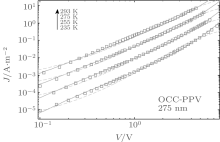 | Fig. 2. Experimental (symbols)[38, 39] and theoretical (dashed lines: Gaussian DOS; solid lines: new DOS) J– V curves at different temperatures of an OC1C10-PPV hole only diode, with thickness L = 275 nm. |
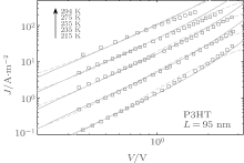 | Fig. 3. Experimental (symbols)[31, 32] and theoretical (dashed lines: Gaussian DOS; solid lines: new DOS) J– V curves at different temperatures of a P3HT hole only diode, with thickness L = 95 nm. |
In Tables 1 and 2, we list six temperature-independent parameters for the ME model by using Gaussian and new DOSs, respectively, including N0, σ , Evf = Ev − EF, Emv = Em − Ev, Wleft, and Wright. The values of σ based on Gaussian DOS are too large as compared with those in Refs. [4] and [6], but are reasonable for the new DOS. Values of Evf are always negative for four materials, which implies the assumption that free holes are non-degenerate used in derivation of Eq. (7) is reasonable. The positive values of Emv show that the levels of ME are higher than the valence levels Ev. The values of Wright are larger than Wleft for the new DOS, which means that the positive built-in potential, Vbi = Wright− Wleft, is reasonable. However, values of Wright in OCC and P3HT for Gaussian DOS are smaller than Wleft for the Gaussian DOS, which means that the built-in potential is negative and unreasonable.
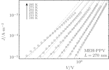 | Fig. 4. Experimental (symbols)[39, 40] and theoretical (dashed lines: Gaussian DOS; solid lines: new DOS) J– V curves at different temperatures of an MEH hole only diode, with thickness L = 270 nm. |
| Table 1. Temperature-independent parameters of mobility edge model with Gaussian DOS optimized by fitting J– V data for NRS, OCC, P3HT, and MEH organic diodes. |
| Table 2. Temperature-independent parameters of the mobility edge model with new DOS optimized by fitting J– V data for NRS, OCC, P3HT, and MEH organic diodes. |
| Table 3. Temperature-dependent mobility values with Gaussian DOS optimized by fitting J– V data for NRS, OCC, P3HT, and MEH organic diodes. |
| Table 4. Temperature-dependent mobility values with new DOS optimized by fitting J– V data for NRS, OCC, P3HT, and MEH organic diodes. |
In Tables 3 and 4, we list the values of temperature-dependent parameter μ 0 for the ME model by using the Gaussian and new DOSs, respectively. These data can be fitted by using the following Arrhenius relationship

In Figs. 5 and 6, we plot the variations of μ 0 with temperature for the four materials, we also plot the smoothed curves by using Eq. (21). It can be seen that the smoothed curves can fit the data points satisfactorily.
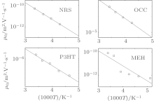 | Fig. 5. Variations of μ 0(T) with temperature for the ME model with Gaussian DOS smoothed by using Eq. (21). |
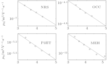 | Fig. 6. Variations of μ 0(T) with temperature for the ME model with new DOS smoothed by using Eq. (21). |
In this work, we simplify the mobility edge (ME) model with a single Gaussian DOS based on recent experimental results about the validity of the traditional Einstein relationship. The free holes are treated as being non-degenerate, and the trapped holes are dealt with as being degenerate. This treatment is confirmed by applying the model to four materials, and also enables the non-complete Gaussian integral for the trapped holes to be easily realized in program. The J– V curves are obtained through solving drift– diffusion equations. With applying the model to four organic diodes, the obvious deviation between theoretical curves and experimental data is observed. In order to solve this problem, a new DOS with exponential tail is proposed. The results show that the agreement of J– V curves with experimental data based on new DOS is far better than that based on the Gaussian DOS. The variation of extracted mobility with temperature can be well described by the Arrhenius relationship.
| 1 |
|
| 2 |
|
| 3 |
|
| 4 |
|
| 5 |
|
| 6 |
|
| 7 |
|
| 8 |
|
| 9 |
|
| 10 |
|
| 11 |
|
| 12 |
|
| 13 |
|
| 14 |
|
| 15 |
|
| 16 |
|
| 17 |
|
| 18 |
|
| 19 |
|
| 20 |
|
| 21 |
|
| 22 |
|
| 23 |
|
| 24 |
|
| 25 |
|
| 26 |
|
| 27 |
|
| 28 |
|
| 29 |
|
| 30 |
|
| 31 |
|
| 32 |
|
| 33 |
|
| 34 |
|
| 35 |
|
| 36 |
|
| 37 |
|
| 38 |
|
| 39 |
|
| 40 |
|


