Corresponding author. E-mail: chenzy@buaa.edu.cn
Corresponding author. E-mail: zhcheng@iphy.ac.cn
Project supported by the National Basic Research Program of China (Grant Nos. 2011CB921801 and 2012CB933102), the National Natural Science Foundation of China (Grant Nos. 11374350, 11034004, 11274361, 11274033, 11474015, and 61227902), and the Research Fund for the Doctoral Program of Higher Education of China (Grant No. 20131102130005).
A planar Hall effect (PHE) is introduced to investigate the magnetization reversal process in single-crystalline iron film grown on a Si (001) substrate. Owing to the domain structure of iron film and the characteristics of PHE, the magnetization switches sharply in an angular range of the external field for two steps of 90° domain wall displacement and one step of 180° domain wall displacement near the easy axis, respectively. However, the magnetization reversal process near the hard axis is completed by only one step of 90° domain wall displacement and then rotates coherently. The magnetization reversal process mechanism near the hard axis seems to be a combination of coherent rotation and domain wall displacement. Furthermore, the domain wall pinning energy and uniaxial magnetic anisotropy energy can also be derived from the PHE measurement.
The properties of magnetic thin films grown on silicon have been investigated by amounts of work in the past decades, because of their applications in the integration of magnetic devices in silicon technology and new opportunities in spintronics, [1, 2] especially the magnetization reversal process of iron films.[3– 5] For an Fe (001) film, the domain wall displacement always dominates the magnetization reversal process and sometimes coherent rotation will participate in the reversal process in a high external field or near the easy axis of film.[6, 7] The magneto-optic Kerr effect (MOKE) is always one of the prior choices to explore the detailed information, but the complicated optical path restricts its application in micro-devices. At the same time, the transport measurement has been developed for decades and has widely been used in silicon-based devices.[8, 9] So it is necessary to investigate the magnetization reversal process of Fe/Si (001) film by the planar Hall effect (PHE).
In our previous work, the MOKE was chosen to investigate the domain wall displacement process of Fe/Si (001) film. Different domain wall displacement processes can be induced in one hysteresis loop with a weak bias field.[10] Furthermore, we find that the magnetization reversal process of Fe/Si (001) film has been proved to be the combination of coherent rotation and domain wall displacement when the external field is smaller than the anisotropy field by torque measurement with anisotropic magnetoresistance.[11] In the present work, the 40-ML single crystal iron film is reported to be grown on a vicinal Si (001) substrate using a flat ultrathin c(2 × 2) iron silicide seed layer and the PHE is used to investigate the magnetization reversal process and determine the domain wall pinning energy. The magnetization reversal process is found to be dominated by different mechanisms at different external field angles. The fitting results of domain wall pinning energy by planar Hall resistance (PHR) show good consistency with the theoretical model.
The sample was grown on a Si (001) substrate using an ultrahigh vacuum molecular beam epitaxial (MBE) chamber equipped with low-energy electron diffraction (LEED). The Si (001) substrate was first well baked out and then flashed, and the well-fined Si (001)-2× 1 surface was obtained.[12] Then, the buffer layer was deposited on the wafer by e-beam bombardment with 2 ML of Fe (99.999% purity), and annealed at 550 ° C for 5 minutes.[13] This procedure gives a highly ordered 2× 2 periodic iron silicide structure to prevent the Fe/Si intermixing. The 40-ML Fe film was deposited on the iron silicide template. The epitaxial relationships among the Fe layer, the iron silicide template, and the Si (001) substrate are as follows:[13, 14] Fe(001)∥ c(2 × 2)FeSi2(001)∥ Si (001) and Fe [100]∥ c(2 × 2)FeSi2[010]∥ Si[110]. A nonmagnetic Cu layer with a thickness of 25 ML was deposited on the sample as a capping layer to protect the sample from being oxidized. In the process of growth, the base pressure was around 2 × 10− 10 mbar (1 bar = 105 Pa) and the substrate was kept at room temperature. After the MOKE measurements, photolithography was used to etch the sample into an 8-probe Hall geometry with the long axis oriented along the Fe [110] axis. The PHR was measured in the direction perpendicular to the current and the current applied to the sample was 5 mA.
Figure 1(a) shows the coordinate system used in MOKE and PHE measurements. The current flows in the Fe [110] direction, so that the PHE effect can obtain its maximum or minimum value at an easy axis where the magnetization prefers to stay. We measure the Hall voltage Vxy perpendicular to the current direction to calculate the PHR. θ and φ are the angles of magnetization and external field with respect to the Fe [100] axis direction, respectively. Figure 1(b) shows the LEED pattern of the iron film grown on the Si (001) substrate. The sharp cubic symmetric spots of the LEED pattern indicate the bcc structure iron film with a thickness of 40 ML.[12, 15]
 | Fig. 1. (a) Coordinate system used in MOKE and PHE measurements, and (b) LEED pattern of 40-ML iron film grown on a Si (001) substrate. |
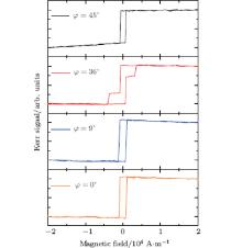
The hysteresis loops of the Fe/Si (001) film are first measured by MOKE. Figure 2 shows the typical hysteresis loops at external field angle φ = 0° , 9° , 36° , and 45° , respectively. The loop at φ = 0° is a typical 1-jump magnetization reversal process induced by 180° domain wall displacement, and the hysteresis loop at φ = 36° is a typical 2-jump magnetization reversal process induced twice by 90° domain wall displacement, respectively.[16] The slight unsymmetry of the loop may be induced by the influence of the weak field from the surroundings.[10] Though the hysteresis loop at φ = 0° seems to be saturated and the one at φ = 45° seems to be hard to reach saturation, they both show the 1-jump magnetization reversal process. They should have different meanings, because the directions of the external field are at the easy axis and hard axis, respectively. Furthermore, we cannot judge whether the loop at φ = 9° is a 1 or 2-jump magnetization reversal process. Apparently, the magnetization almost stays near the easy axis, because the loops do not show any coherent rotation information and the easy axis is the minimum energy position of the system. When φ = 9° and the external field reaches a positive maximum, the magnetization stays in the Fe [100] direction. As the external field decreases, the magnetization jumps to the Fe


 | Fig. 2. Typical hysteresis loops of the Fe/Si (001) film, measured by MOKE at external field angle φ = 0° , 9° , 27° , 36° , and 45° , respectively. |
In a single crystalline system, the PHR can be expressed as[9]

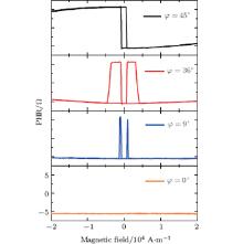
Unlike the MOKE measurement, the variation of the PHR value is twice as fast. That is to say, the PHR reaches its minimum value in the Fe [100] or Fe 


 | Fig. 3. Typical PHE curves at external field angle φ = 0° , 9° , 27° , 36° , and 45° , respectively. |
As the thin film epitaxially grows on substrates, it may induce a weak uniaxial magnetic anisotropy (UMA) because of the stress, lattice mismatch or other effects.[18– 20] Here, we consider the first cubic magnetocrystalline anisotropy (MCA), the UMA, and the Zeeman energy for Fe/Si (001) film. In general, the orientation of the UMA can be along any direction, so we separate it into two components: Ku1 along Fe [100] and Ku2 along Fe [110].[21] The total free energy density of the system with an external field H is described as


where the first and the second terms are the UMA energies along the directions [100] and [110], respectively. The third term is the first cubic MCA energy. The fourth term is the Zeeman energy of external fieldH. Ku1 and Ku2 are the UMA constants and K1 is the first cubic MCA constant. M is the saturation magnetization of iron.
The magnetization will always rotate to a local minimum energy E(θ ) for a given field when it obeys the Stoner– Wohlfarth model. However, the magnetization will be unpinned and switched to another local minimum energy due to the existence of domain structure.[22, 23]
In the previous work, the UMA in Fe/Si (001) is very small compared with the MCA and the domain wall pinning energy.[10, 11] Due to the existence of Ku2, the local minima position will shift a small angle δ , so we set the local minima of Eq. (2) to be at θ = − δ , 90° + δ , 180° − δ , and 270° + δ , where 
For the 1-jump process,

and for the 2-jump process,


where ε 90° − 2δ , ε 90° + 2δ , and ε 180° are the pinning energies for the 2-jump and 1-jump magnetization reversal process.
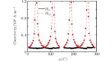
For other ranges of φ we can calculate the coercivity expressions in different ranges of external fields by changing the angle in steps of 45° . Figure 4 shows the fitting results of Eqs. (4) and (5) from the PHE measurement. As the PHE can only show the coercivity of the 90° domain wall displacement process, no coercivity is induced by the 180° domain wall displacement. It is an excellent correspondence between theoretical calculations and experimental measurements. Also, we can calculate the domain wall pinning energies ε 90° − 2δ /μ 0M = 1.03 × 10³ A/m, ε 90° + 2δ /μ 0M = 1.15 × 10³ A/m, δ = − 0.5° , and Ku1/μ 0M = − 80 A/m. We can also calculate the domain wall pinning energy from the hysteresis loops from the MOKE measurement, which is consistent with the one from the PHR measurement, and ε 180° /μ 0M = 1.83 × 10³ A/m. As predicted in Ref. [16], 2ε 90° > ε 180° will induce a 1-jump magnetization reversal process in a certain angular range, and this range depends on how much greater than ε 180° the 2ε 90° is. Here, the values of 2ε 90° − 2δ and 2ε 90° + 2δ have no big difference from ε 180° , which explains why there exists so wide an angular range of the 2-jump switching process.
In this paper, we investigate the magnetization reversal process of 40-ML iron films grown on Si (001) substrates. The MOKE measurement shows typical 90° and 180° domain wall displacements when scanning the external field. However, the linear feature of MOKE measurement leads to an indistinct area between these two domain wall displacements at certain external field angles. The PHE overcomes this shortage, and shows clearly the magnetization reversal process. Especially, there are both coherent rotation and domain wall displacement near the hard axis. The domain wall pinning energy and UMA can also be determined accurately from the MOKE and PHE measurements.
| 1 |
|
| 2 |
|
| 3 |
|
| 4 |
|
| 5 |
|
| 6 |
|
| 7 |
|
| 8 |
|
| 9 |
|
| 10 |
|
| 11 |
|
| 12 |
|
| 13 |
|
| 14 |
|
| 15 |
|
| 16 |
|
| 17 |
|
| 18 |
|
| 19 |
|
| 20 |
|
| 21 |
|
| 22 |
|
| 23 |
|
| 24 |
|
| 25 |
|
| 26 |
|


