Ordered silicon nanorod arrays with controllable geometry and robust hydrophobicity*
Cite this Article
Wang Zi-Wen, Cai Jia-Qi, Wu Yi-Zhi, Wang Hui-Jie, Xu Xiao-Liang. Ordered silicon nanorod arrays with controllable geometry and robust hydrophobicity* . Chinese Physics B, 2014, 24(1): 017802 
Permissions
Ordered silicon nanorod arrays with controllable geometry and robust hydrophobicity*
Corresponding author. E-mail: xlxu@ustc.edu.cn
Project supported by the National Natural Science Foundation of China (Grant No. 51272246) and the Scientific and Technological Research Foundation of Anhui Province, China (Grant No. 12010202035).
Abstract
Highly ordered silicon nanorod (SiNR) arrays with controllable geometry are fabricated via nanosphere lithography and metal-assisted chemical etching. It is demonstrated that the key to achieving a high-quality metal mask is to construct a non-close-packed template that can be removed with negligible damage to the mask. Hydrophobicity of SiNR arrays of different geometries is also studied. It is shown that the nanorod structures are effectively quasi-hydrophobic with a contact angle as high as 142°, which would be useful in self-cleaning nanorod-based device applications.
Keyword:
78.67.Qa; 68.08.Bc; silicon nanorod array; hydrophobicity; self-cleaning; metal-assisted chemical etching
1. Introduction
Silicon nanorods (SiNRs) have drawn great interest in recent years due to their exciting applications in numerous fields of research such as field effect transistors (FETs), [1– 4] biological and chemical sensors, [5– 9] and photovoltaics (PVs).[10– 15] Various methods have been developed for fabricating SiNRs, including vapor-liquid-solid (VLS) growth, [16– 18] oxide assisted growth (OAG), [19– 21] reactive ion etching (RIE), [22– 24] and metal-assisted chemical etching (MACE).[25– 30] Among these methods, MACE is undoubtedly the most promising approach to large-scale fabrication of SiNRs, due to its low cost and high output. Huang et al. combined MACE with nanosphere lithography to create ordered SiNR arrays, .[26] but their fabrication of MACE templates involves reactive ion etching, which is presently too costly for mass production. Peng et al.adopted a sintering and chemical etching method in fabricating MACE templates, [25] which is much more cost-effective, and therefore more suitable for industrial applications. However, due to lack of control over the process variables, the geometry of the nanorods was uncontrollable in their case.
In this work, we investigate the key factors for controlling this sintering and etching process and obtain SiNR arrays with controllable geometries, i.e., controllable diameter, length and filling factor of the nanorods. Moreover, the hydrophobicity of SiNR arrays with different geometries is also studied, where the Cassie model[31] is adopted for quantitative analysis. With a contact angle as high as 142° , the quasi-hydrophobicity can be useful in the application of self-cleaning nanorod-based devices.
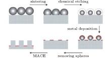
A schematic of the fabrication process appears in Fig. 1. In brief, close-packed (CP) monolayer silica nanosphere templates are sintered and chemically etched to form non-close packed (NCP) templates. Noble metal is deposited on the sample and then the silica nanospheres are ultrasonically removed, leaving a continuous metal film with periodic nanoholes. The metal film is then used as the mask for MACE, thus creating the ordered SiNR arrays.
 | Fig. 1. Schematic of our proposed fabrication process for SiNR arrays. |
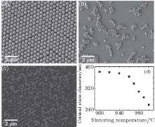
Chemical reagents such as HF (49%), H2O2 (30%), HCl (36%– 38%), and HNO3 (65%) were purchased from the Sinopharm Chemical Reagents Corporation and used without further purification. All the reagents are analytically pure. The Si(100) wafers has resistivity of 7– 14 Ω · cm and thickness of 500 μ m. They were p-type and boron-doped. Monolayer silica nanosphere templates were prepared via the slope self-assembly and thermal treatment methods described by Wu et al.[32] In brief, silicon substrates were tilted at a certain angle and then covered with latex in an oven at 45 ° C. Figure 2(a) shows a typical SEM image of the as-prepared templates. By using monodisperse silica nanospheres of different diameters, CP templates with different lattice constants can be readily prepared; CP templates with a lattice constant of a = (0.54± 0.01) μ m were used for further treatment throughout this work unless otherwise stated. All the nanostructures were examined by a field emission scanning electron microscope (SEM, JSM-6700F) operating at 5 kV.
The as-prepared CP templates were sintered in a muffle furnace for 3 hours at different temperatures. Under the influence of gravity, the softened silica spheres deformed slightly, and their contact areas with the substrate increased. Next, the samples were immersed in 1 mol/L HF solution at 25 ° C to partly dissolve the silica spheres and create NCP templates. The speed at which the sphere diameter decreases was determined to be about a constant of 45 nm/min, which was used to tune the diameter of the spheres. Then, a 10-nm layer of gold was deposited onto the samples using a conventional thermal evaporation method. After that, the samples were ultrasonically treated in DI water (18 MΩ · cm) for 0.5 minutes to remove the silica spheres, leaving the metal film with periodic nanoholes, i.e., the mask for MACE (Fig. 3(a)). As can be seen, the size of silica spheres after chemical etching determines the size of holes on the mask, therefore defining the diameter of the SiNRs.
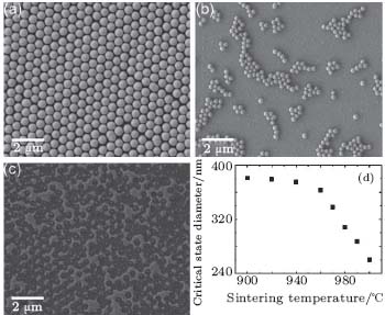 | Fig. 2. (a) Monolayer close-packed colloidal crystal templates prepared via self-assembly and thermal treatment. (b) Silica spheres leaving their original places and repositioning due to excessive etching in HF solution and capillary force, respectively. (c) Large connection area between the spheres and the substrate requires intense ultrasonication, which damages the metal mask. (d) Relationship between sintering temperature and critical sphere diameter. |
However, it is worth noting that the reduced sphere diameter cannot be varied freely, because the connection area between the silica spheres and the substrate also decreases with etching time. If the connection area is totally dissolved, the silica spheres would leave their original place, as shown in Fig. 2(b). On the other hand, if the connection area between the silica spheres and the substrate is larger than needed, more intense ultrasonication is needed to break the connection, which risks destroying the metal mask as shown in Fig. 2(c). Therefore, an optimum condition exists wherein the connection between a sphere and the substrate is just enough to keep the sphere in place. This state will be called the “ critical state” hereafter.
At higher sintering temperatures, the silica spheres soften more and deform more significantly under gravity, so the contact areas between the spheres and the substrate are determined by the temperature. Since the critical-state sphere diameter decreases as the contact area increases, each critical-state sphere diameter corresponds to a different sintering temperature. To investigate this relationship, samples were sintered at different temperatures. SEM images were taken of each sample at small intervals of etching time, to determine whether the silica spheres were still in their original place. Those states where the spheres were about to leave their original place were taken as critical states. Figure 2(d) shows the relationship between sintering temperature and critical sphere diameter. Using this relationship, different sintering temperatures can be predetermined to obtain critical state NCP templates with certain sphere diameters within the temperature range. Note that when the temperature is above approximately 960 ° C, the connection area between silica spheres and the substrate increases more significantly with temperature, which causes the critical sphere diameter to decrease more drastically.
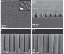
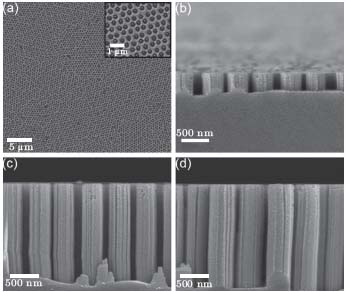 | Fig. 3. (a) Large-area, high-quality metal masks. (b)– (d) Three different SiNR arrays with (b) d1 = 0.34 μ m, l1 = 0.35 μ m, (c) d2 = 0.34 μ m, l2 = 1.68 μ m, (d) d3 = 0.44 μ m, l3 = 1.76 μ m. Samples (b)– (d) are labelled as samples S1– S3 hereafter. |
Figure 3(a) shows a typical mask obtained by ultrasonication of a critical-state NCP template that was deposited with gold. Very weak ultrasonication was needed, so damage to the mask was negligible. The samples were then immersed in oxidizing HF solution (4.4 mol/L HF, 0.9 mol/L H2O2) at 25 ° C for MACE. Finally, the samples were immersed in aqua regia to remove the gold mask. Figures 3(b)– 3(d) show resultant SiNR arrays with different geometries. The sample in Fig. 3(b) was etched for 10 min, and the samples in Figs. 3(c) and 3(d) were etched for 30 min.
Huang et al.[26] demonstrated that the nanorod length is proportional to the etching time. However, we discovered that the etching of the silicon substrate did not start immediately after the samples were immersed in the etching solution in our case. This phenomenon was visually obvious during the etching process because the samples darkened once the etching of the silicon substrate actually began. This can be attributed to the existence of an extra thick oxide layer on the silicon substrate, which is due to sintering at high temperature, and it has to be dissolved before the etching of the substrate's silicon can occur. Therefore, a certain period of time should be deducted from the total immersion time to obtain the effective etching time. Assuming that the length of the SiNRs is proportional to the effective etching time, the following relation holds:
 |
where t0 is the time needed for the oxide layer to be removed, t1 = 10 min and t2 = 30 min are the total etching times for samples S1 and S2, and l1= 0.35 μ m and l2= 1.68 μ m are the lengths of the SiNRs in the two samples. The value of t0 can therefore be determined as t0= 4.7 min, which is in good accord with experimental observations.
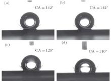
While surface roughness is well known to contribute to water-repellency, quantitative analysis of this phenomenon is usually imprecise due to imperfection of the surface structure.[33– 49] With precisely controllable geometries, the as-prepared SiNR arrays are well suited for such analysis. Therefore, as an add-on, we further investigated the hydrophobicity of the as-prepared SiNR arrays. The same samples (S1– S3) were modified with heptadecafluorodecyl trimethoxysilane, using methods reported by Gong et al.[47] In short, the samples were immersed in a mixture of 2 parts HTMS and 98 parts toluene in terms of volume for 12 hours at room temperature. A vacant silicon substrate (S4) was treated with the same procedure for comparison. Water contact angle measurement was carried out at room temperature using the CAST 2.0 contact angle analysis system (Solon (Shanghai) Information Technology Co., Ltd). Water droplets (2 μ l) were placed at five different positions of each sample and the average value was calculated. Figure 4 shows that the contact angle of the vacant sample (S4) is considerably smaller than that of the structured samples (S1– S3), indicating that the nanostructures contribute significantly to hydrophobicity. Contact angles of S1 and S2 are almost the same, both exceeding 140° , indicating robust hydrophobicity that is independent of SiNR length within the range of aspect ratios studied. In addition, with the array configuration, we can easily tune the filling factor of the nanorods to achieve optimal hydrophobicity. This would be much harder for the un-patterned case, where the initial colloidal crystal templates have to be un-patterned and therefore non-close packed. Moreover, an array configuration of the nanorods is usually desirable in device applications. It is obvious that a hydrophobic nanorod device with an array configuration would be easier to fabricate and model than one without.
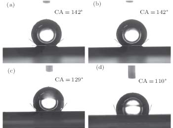 | Fig. 4. Contact angles of SiNR arrays with different geometries. Images (a)– (d) correspond to samples S1– S4, respectively. |
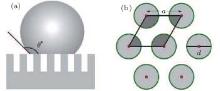
For quantitative analysis, we adopted the Cassie– Baxter model.[31] (Fig. 5(a)). For simplicity, we neglect the sagging of water between the nanorods, which is a reasonable approximation since the filling factor of our nanorod array is relatively large. In this circumstance, the phenomenal contact angle can be calculated using the relationship
 |
where θ e a is the intrinsic contact angle (corresponding to S4), and fs is the ratio of the protruding roof area to the phenomenal contact area. For the hexagonal geometry (Fig. 5(b)), simple calculation gives the following expression of fs:
 |
where d is the diameter of the nanorod, and a is the lattice constant of the hexagonal lattice. The expression of the phenomenal contact angle θ * (Eq. (3)) is independent of the length of the nanorod, which is in accord with the fact that the water contact angle measurements of samples S1 and S2 are approximately the same. The calculated contact angles of samples S1, S2, and S3 are 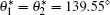

 | Fig. 5. (a) Schematic of Cassie model. θ * is the phenomenal contact angle. (b) Schematic of the top-down view of the nanorod arrays. The diameter of the nanorod is d and the lattice constant of the hexagonal lattice is a. The unit cell of the hexagonal lattice is chosen as the parallelogram. fs can be calculated as the ratio of the deep dark area to the unit cell area. |
In conclusion, we fabricated SiNR arrays with controllable geometries, especially the diameter and length of the nanorods. Moreover, we demonstrated that constructing critical-state non-close-packed templates is the crux of obtaining high-quality metal masks during SiNR arrays fabrication via nanosphere lithography and metal-assisted chemical etching. Additionally, we studied the hydrophobicity of SiNR arrays of different geometries. With the array configuration, which is usually desirable in device applications, the filling factor of the nanorods can be easily tuned to achieve optimal hydrophobicity. Therefore, they might be exploited for self-cleaning applications in SiNR-based devices.
We thank Hao Jia and Jianfa Chen for their assistance.
Reference
| 1 |
|
| 2 |
|
| 3 |
|
| 4 |
|
| 5 |
|
| 6 |
|
| 7 |
|
| 8 |
|
| 9 |
|
| 10 |
|
| 11 |
|
| 12 |
|
| 13 |
|
| 14 |
|
| 15 |
|
| 16 |
|
| 17 |
|
| 18 |
|
| 19 |
|
| 20 |
|
| 21 |
|
| 22 |
|
| 23 |
|
| 24 |
|
| 25 |
|
| 26 |
|
| 27 |
|
| 28 |
|
| 29 |
|
| 30 |
|
| 31 |
|
| 32 |
|
| 33 |
|
| 34 |
|
| 35 |
|
| 36 |
|
| 37 |
|
| 38 |
|
| 39 |
|
| 40 |
|
| 41 |
|
| 42 |
|
| 43 |
|
| 44 |
|
| 45 |
|
| 46 |
|
| 47 |
|
| 48 |
|
| 49 |
|