
Structures and electrical properties of pure and vacancy-included ZnO NWs of different sizes
[Yu Xiao-Xiaa) , Zhou Yana) , Liu Jiab) , Jin Hai-Bob) , Fang Xiao-Yong†a)  , Cao Mao-Sheng‡
b) ]
, Cao Mao-Sheng‡]
|
|


†Corresponding author. E-mail: fang@ysu.edu.cn
‡Corresponding author. E-mail: caomaosheng@bit.edu.cn
*Project supported by the National Natural Science Foundation of China (Grant Nos. 51132002 and 11574261) and the Natural Science Foundation of Hebei Province, China (Grant No. A2015203261).
The structures and electronic properties of ZnO nanowires (NWs) of different diameters are investigated by employing the first-principles density functional theory. The results indicate that the oxygen vacancy ( VO) exerts a more evident influence on the band gap of the ZnO NWs. However, the effect will be weakened with the increase of the diameter. In addition, the energy band shifts downward due to the existence of VO and the offset decreases with the reduction of the VO concentration. As the concentration of surface Zn atoms decreases, the conduction band shifts downward, while 2p electrons are lost in the oxygen vacancy, resulting in the split of valence band and the formation of an impurity level. Our findings agree well with the previous observations and will be of great importance for theoretical research based on ZnO NWs.
ZnO is a semiconductor with a direct wide bandgap (3.37 eV) and a large exciton binding energy (60 meV) at room temperature.[1– 3] Some of its features are improved when it is a nanoscale material. ZnO nanowires (ZnO NWs) are one-dimensional structures and are easy to grow along the preferred orientation. In addition, ZnO NWs have strong quantum confinement effects and high specific surface area. The ZnO NWs have aroused intensive research interest in several applications, such as field effect transistors, ultraviolet (UV) lasers, light emitting diodes, energy-conversation devices, solar cells, and microwave absorption.[4– 8] Furthermore, the defects related to ZnO NWs, particularly oxygen vacancy (VO), are analyzed for extensive application, both experimentally and theoretically. In 2009, Wang and Zhang suggested that oxygen anti-site and VO coexisted in ZnO and the visible light emission peak at 2.53 eV disappeared after the sample had been exposed to air or annealed in oxygen ambiance.[9] In 2012, Wong et al.’ s experimental results indicated that the VO defects were not only spatially located on the surface of each NW but also in an annular region beneath the surface as the ZnO NW elongates.[10] In 2013, Seo et al. observed that ZnO nanowire transistors fabricated with ZnO NWs doped with sulfur as a reducing agent exhibited a more stable threshold voltage characteristic under light illumination than nanowire transistors fabricated with pure ZnO nanowires.[11] Although the experimental researches related to VO– ZnO nanowires (oxygen vacancy included ZnO nanowires) are abundant, theoretical studies are rare. In 2001, Chris and Van de Walle believed that the VO was a deep acceptor.[12] He et al.’ s studies provided a basic understanding of the size effect of strength in single crystalline NW and evaluated the dominant factors which may induce scattered fracture strains, such as the effective quantities of atomic vacancies.[13] Wang et al. predicted that the VO caused a blue shift for the increased dielectric peak.[14] In 2014, Deng et al. investigated the migration of VO in ultra-thin ZnO nanowires.[15] Wu et al. investigated the magnetic properties of defects-including materials and indicated that the single Zn defect could induce a large local magnetic moment (∼ 2 μ B) in the ZnO nanowires in 2015.[16]
In this paper, we investigate the models of ZnO NWs with three different diameters and discuss the influences of VO on the structures of ZnO NWs. Primarily, the six hexagonal cross sectional structures are constructed based on the lattice structure of ZnO primitive cell. Further simulations are carried out to systematically analyze the electronic properties. Our research is helpful for understanding the defects, particularly VO, in ZnO NWs and are of great technological importance for developing the ZnO NWs-based devices in photocatalysis and optoelectronics.
Our first-principle calculations are carried out by density function theory (DFT) and implemented in the DMol3 package in Material Studio (MS) software. The generalized gradient approximation (GGA) and Perdew and Wang 91 (PW91) are utilized to approximate the exchange-correlation potential. The DFT semi-core pseudo-potential is used to describe the interactions between ions and electrons (O-2s22p4, Zn-3d104s2). The GGA + U is used for the strong correlation effects of d and f state electrons in the calculation but it is not suitable for the filled shell, such as the d state electrons in zinc atoms. Based on the pseudo-potential plane wave basis set double numerical plus polarization (DNP) and the one-dimensional periodic boundary condition, the multi-electronic system is described with a plane wave function. The k-point is set to be 1 × 1 × 4 under the Monkhorst– Pack scheme.
First, get rid of the redundant atoms of the wurtzite structure ZnO supercell, which is obtained from the library source structure file in order to establish the structures of ZnO NWs of three different circumscribed circle diameters. The VO– ZnO NWs are obtained by removing one of the three-bond O atoms on the same layer based on the ZnO NWs structures with different dimensions. The dangling bonds of the three nearest Zn atoms are also cut. A vacuum region along the [0001] direction is added to the structures, which ensures that the structures nearby do not interact with each other. The structures are then adequately relaxed and the optimization may be finished if the convergence criteria are fully satisfied.
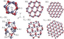
ZnO has a typical hexagonal wurtzite crystalline structure and the hexagonal ZnO NWs has the minimum cohesive energy; namely, they are the most stable structures.[17] Furthermore, the most stable location for VO in ZnO NW is on the surface.[18] Therefore, we focus on the cases of the native and the VO– ZnO NWs with a hexagonal cross section. The hexagonal cross shape NWs are denoted as H1 (12 atoms/cell), H2 (48 atoms/cell), H3 (108 atoms/cell), and the homologous NWs with VO are denoted as VO– H1 (11 atoms/cell), VO– H2 (47 atoms/cell), and VO– H3 (107 atoms/cell), respectively.
The pure and the VO– ZnO NWs with three different diameters are considered, which are represented in Fig. 1.
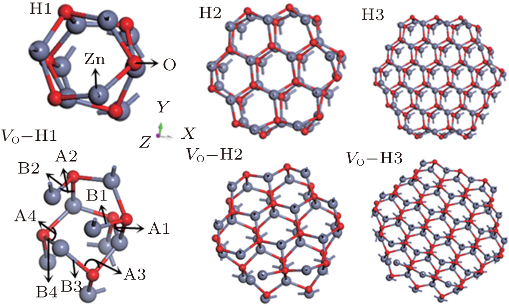 | Fig. 1. Crystal structures of H1, H2, H3, VO– H1, VO– H2 and VO– H3: the small and the big ball represent oxygen and zinc atoms, respectively, as shown in Fig. 1; the position of bonds and angles are indicated in the structure of VO– H1 and the bonds and angles are at similar sites in other structures in the uniform direction. |
In each case, the structure is fully relaxed and the corresponding parameters, such as the crystal constant c, diameter, bond length, bond angle and total energy, are listed in Table 1. The average relaxed diameter is defined with respect to the position of oxygen atoms at the sub-surface.
The stability of the pure hexagonal ZnO NWs decreases with the diminution of diameter and the pure ZnO NWs are more stable than the VO– ZnO NWs, as shown in Table 1. The increasing rates of stability are 3.80%, 0.95%, and 0.42%, respectively, which indicates the stability of VO– ZnO NWs increases as the VO concentration reduces.
| Table 1. Structure parameters of the pure and the VO– ZnO NWs. The last three columns give the differences between H1 and VO– H1 (Δ H1), H2 and VO– H2 (Δ H2), H3 and VO– H3(Δ H3), respectively. |
The Zn– O bond length and the angle Zn– O– Zn nearest to VO are marked as Bi and Ai (i = 1, 2, 3 and 4) at four different specific positions of six studied cases, respectively, as shown in Fig. 1. The following conclusions are drawn from Fig. 1 and Table 1.
1) The Zn– O bond lengths of B1, B2, and B4 and the Zn– O– Zn angles of A1, A2, and A3 decrease with the reduction of diameter for pure ZnO NWs due to the added atoms, respectively. Likewise, the B1, B2, B4 and the A1, A2, A3 of VO– ZnO NW display the same scenarios as those for pure ZnO NWs.
2) The Zn– O– Zn angles of VO– ZnO NWs are smaller than those of intrinsic ZnO NWs, and the average Zn– O bond lengths in VO– ZnO NWs are longer than in the pure NWs, which means the interaction between Zn and O atoms turns stronger in the cases of VO– ZnO NWs, as shown in Table 1. However, the growth rate of bond length of B1 increases while that of B3 reduces, which means that the zinc atom in B1 moves outward and the oxygen atom in B3 moves inward with increasing size.
3) Removing one of the oxygen atoms leads to the three Zn atoms increasingly growing closer. For example, the average distances between the three Zn atoms nearest to VO in VO– H1, VO– H2, and VO– H3 are 2.576 Å , 2.579 Å , and 2.582 Å , respectively, which increase with the growing diameter and favor molecular adsorption. Furthermore, although the distance of Zn– O at surface increases slightly with the rising of diameter, no clear trend can be observed at the sub-surface.
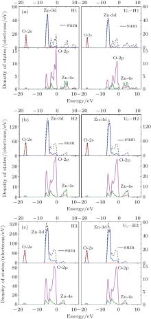
The electronic density of states (DOS) and band structures of all the studied cases are shown in Figs. 2 and 3. As is well known, the correlation interaction between excited electrons in the calculating model is underestimated, but the tendency of the band gap can be predicted by our results.
The following conclusions are drawn from Figs. 2– 4.
(i) In the lowest portion of valence band (– 18.0 eV– 16.0 eV), there is a peak from O-2s electronic contribution. At the lower portion of valence band (– 7.0 eV– 4.0 eV), the notable peaks consist of the peak from Zn-3d state, which is dominant, and the slight peak from O-2p state; the two states display contrary scenarios at the upper portion of the valence band (– 4.0 eV– 0 eV). It is the cooperation of Zn-4s and O-2p states that constitutes the conduction band of pure ZnO and VO– ZnO NWs.
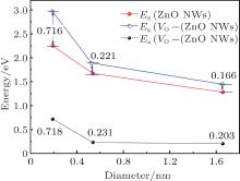
(ii) The pure ZnO NWs are direct-band-gap semiconductors, and the values of band-gap Eg (the energy difference between conduction band minimum (CBM) and valence band maximum (VBM)) of H1, H2, and H3 are 2.249 eV, 1.670 eV, and 1.282 eV, respectively. The results accord with the previous calculations by Haffad et al.[19] Obviously, band gap decreases with the increase of the diameter, as indicated in Fig. 4. The energy band of ZnO NWs also exhibits pronounced symmetry and the conduction band is a quasi-sp energy band due to the approximating parabolic shape.
Similarly, VO– ZnO NWs are direct-band-gap semiconductors, and the values of band-gap Eg of VO– H1, VO– H2, and VO– H3 are 2.965 eV, 1.891 eV, and 1.448 eV, respectively. Namely, the larger the size, the smaller the band gap is, as can be seen in Fig. 4. The electronic states are redistributed because of the removal of one oxygen atom, which introduces the defect level[20] into the gap.
(iii) In addition, the defect energy level is close to the VBM, which is responsible for the acceptor energy level (the ionization energy Ea is shown in Table 2). The ZnO NWs are appointed as good candidates in applications for optoelectronic nanodevices[21] because of their novel characteristics, whereas it is extremely difficult for VO– ZnO NWs to be used in p-type high conductivity equipment.
(iv) The CBM shifts downward slightly with the increase of diameter, as shown in Fig. 3. However, the downward shift of the valance band in VO– ZnO NWs shows that the Fermi level approaches upward, and the percentages of movement are 0.20%, 0.85%, and 1.68% with the increase of size, respectively.
As is displayed in Fig. 4 and Table 2, zinc atoms play a dominant role in the CBM. For ZnO NWs, the CBM shifts downward notably, as discussed above, because the nsz decreases sharply as the diameter increases. The CBM of VO– ZnO NWs presents the same scenario. The Fermi level is the VBM for ZnO NWs, which is determined mainly by no rather than nso. However, no of VO– ZnO NWs reduces with the augment of size, demonstrating that the position of VBM in VO– H3 is highest, which is consistent with the discussion above.
(v) The effective mass value of hole is defined by using the formula of solids physics:
For the native ZnO NWs, the effective mass value of hole increases with the increasing size in the [0001] direction because of the enhancement of localization of electron states in larger size ZnO NWs, as illustrated in Fig. 3. Furthermore, the VO experiences an intensive influence on the energy level because the charges at the surface are redistributed for the existence of VO and are bounded around it. The effective mass value of the defect level in VO– ZnO NW increases with the diminution of diameter in the uniform orientation. As is well known, the defect is caused by the oxygen vacancy and the vacancy concentration reduces notably from VO– H1 to VO– H3. It is reasonable to believe that the vacancy concentration exerts an influence on the effective mass value of the defect level in VO– ZnO NW. The higher the concentration, the larger the effective mass values of holes are, which can be seen in Table 2.
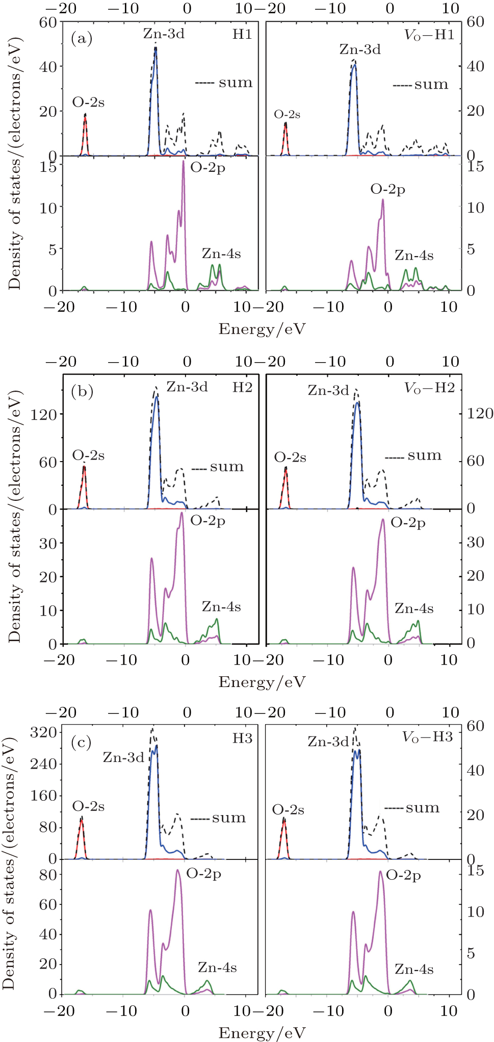 | Fig. 2. Densities of states of the six cases under study: (a) H1 and VO– H1, (b) H2 and VO– H2, (c) H3 and VO– H3. |
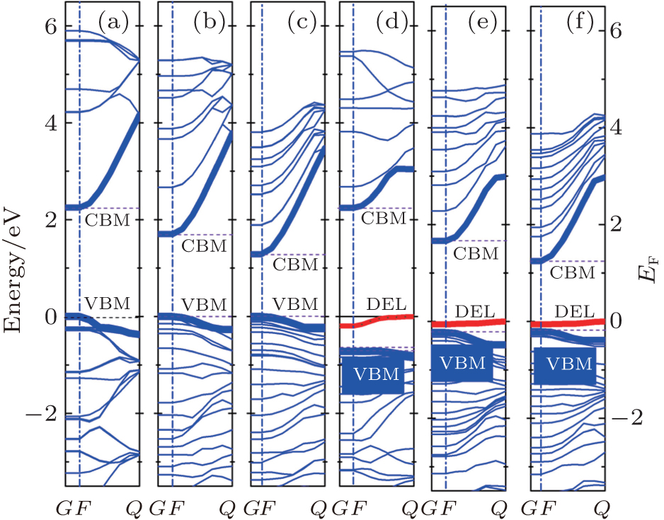 | Fig. 3. Band structures of ZnO and VO– ZnO NWs: (a) H1, (b) H2, (c) H3, (d) VO– H1, (e) VO– H2, and (f) VO– H3. F → Q is the [0001] direction, Fermi level is set to zero. Besides, CBM and VBM represent the conduction band minimum and the valence band maximum, respectively; DEL represents defect level. |
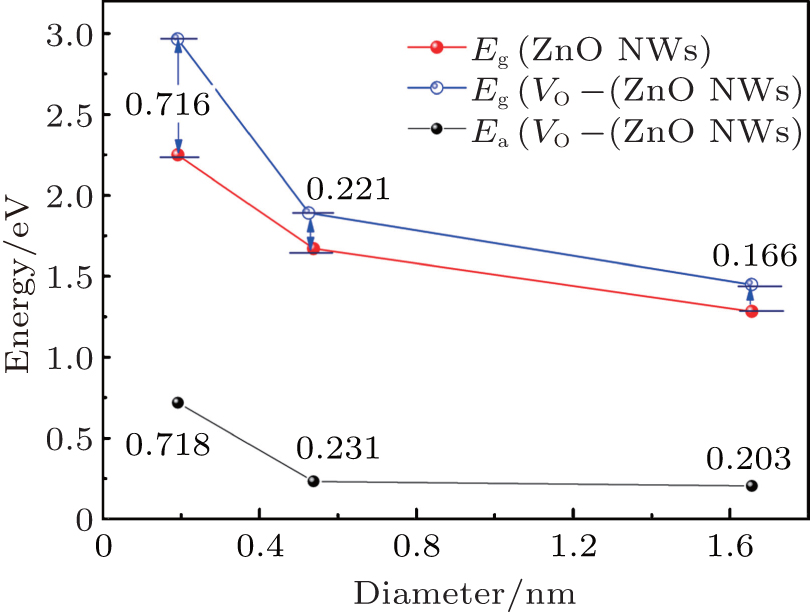 | Fig. 4. Size- dependent band structures of ZnO and VO– ZnO NWs. |
| Table 2. Calculated parameters of the pure and the VO– ZnO NWs. |
In this work, we investigate the effects of the oxygen vacancy on the electronic properties of hexagonal cross section ZnO NWs of different sizes. Utilizing the density function theory, we find that the band gap Eg of VO– ZnO NWs decreases with the diminution of Vo concentration. Nonetheless, the shape of band edges remains unchanged. VO obviously enhances the locality of electron state in the valance band. The effective mass value of the hole changes a lot with the difference of nso, which increases the cost of p-type ZnO synthesis. In addition, the energy bands of VO– ZnO NWs shift downward. Therefore, we argue that VO is a shallow acceptor for ZnO NWs.
| 1 |
|
| 2 |
|
| 3 |
|
| 4 |
|
| 5 |
|
| 6 |
|
| 7 |
|
| 8 |
|
| 9 |
|
| 10 |
|
| 11 |
|
| 12 |
|
| 13 |
|
| 14 |
|
| 15 |
|
| 16 |
|
| 17 |
|
| 18 |
|
| 19 |
|
| 20 |
|
| 21 |
|