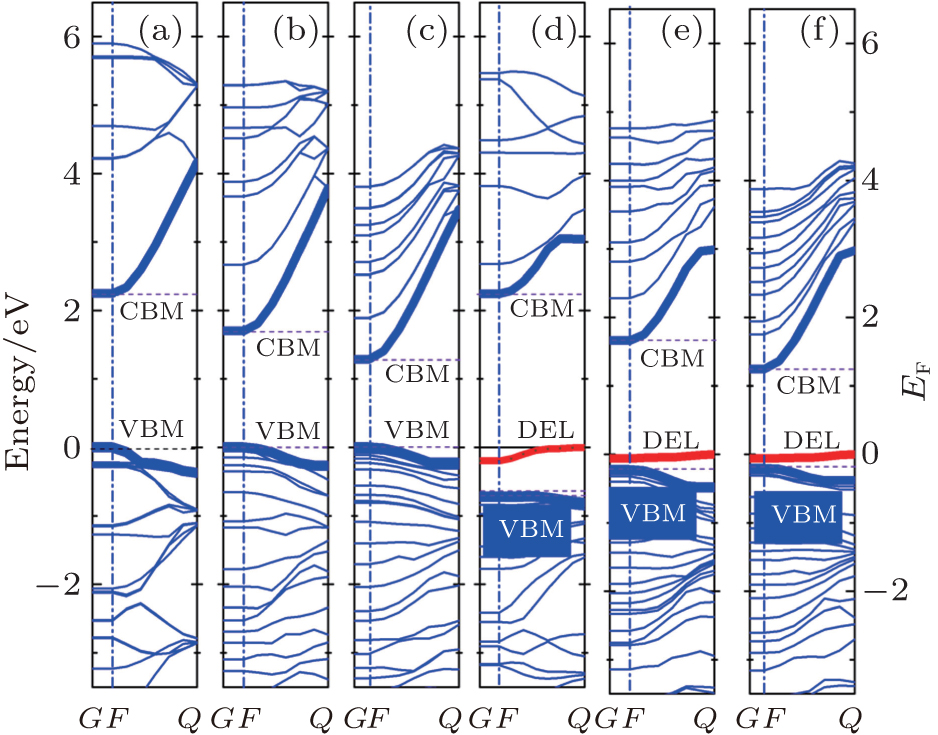
Structures and electrical properties of pure and vacancy-included ZnO NWs of different sizes
Yu Xiao-Xiaa), Zhou Yana), Liu Jiab), Jin Hai-Bob), Fang Xiao-Yong†a), Cao Mao-Sheng‡b)
       
Band structures of ZnO and V O–ZnO NWs: (a) H1, (b) H2, (c) H3, (d) V O–H1, (e) V O–H2, and (f) V O–H3. F → Q is the [0001] direction, Fermi level is set to zero. Besides, CBM and VBM represent the conduction band minimum and the valence band maximum, respectively; DEL represents defect level.