Hysteresis loop behaviors of ferroelectric thin films: A Monte Carlo simulation study*
[Bedoya-Hincapié C. M.a), b)  , Ortiz-Álvarez H. H.
a), c) , Restrepo-Parra E.a) , Olaya-Flórez J. J.d) , Alfonso J. E.e) ]
, Ortiz-Álvarez H. H.|
|

 , Ortiz-Álvarez H. H.
†Corresponding author. E-mail: cmbedoyahi@unal.edu.co
*Project sponsored by the research departments of the Universidad Nacional de Colombia DIMA and DIB under Project 201010018227-“Crecimiento y caracterización eléctrica y estructural de películas delgadas de BixTiyOz producidas mediante Magnetrón Sputtering” and Project 12920-“Desarrollo teóricoexperimental de nanoestructuras basadas en Bismuto y materiales similares” and “Bisnano Project.”
The ferroelectric response of bismuth titanate Bi4Ti3O12 (BIT) thin film is studied through a Monte Carlo simulation of hysteresis loops. The ferroelectric system is described by using a Diffour Hamiltonian with three terms: the electric field applied in the z direction, the nearest dipole–dipole interaction in the transversal ( x– y) direction, and the nearest dipole–dipole interaction in the direction perpendicular to the thin film (the z axis). In the sample construction, we take into consideration the dipole orientations of the monoclinic and orthorhombic structures that can appear in BIT at low temperature in the ferroelectric state. The effects of temperature, stress, and the concentration of pinned dipole defects are assessed by using the hysteresis loops. The results indicate the changes in the hysteresis area with temperature and stress, and the asymmetric hysteresis loops exhibit evidence of the imprint failure mechanism with the emergence of pinned dipolar defects. The simulated shift in the hysteresis loops conforms to the experimental ferroelectric response.
Lead-free ferroelectric materials have attracted the attention of researchers seeking candidate materials that are environmentally friendly and exhibit high polarizations and low fatigue effects. In this respect, bismuth titanate (Bi4Ti3O12, BIT), a bismuth layer-structured ferroelectric (BLSF) that belongs to the Aurivillius family, [1] has been studied due to its ferroelectric, piezoelectric, and pyroelectric properties over a wide range of temperatures, up to 948 K.[2, 3] The Aurivillius ceramics are known for their significant remnant polarization (Pr, low coercive field (Ec, excellent fatigue characteristics, and high Curie temperature.[4, 5] In particular, for the best performance of ferroelectric random access memory applications, it is desirable to have a square and symmetric hysteresis (P– E) loop, a long endurance, and a low leakage current.[6] Experimentally, the characteristic shape of the loop is very sensitive to the type of electrode employed, the interface between the film and the electrode, the temperature, stress, and the presence of point defects such as oxygen vacancies.[7] For instance, the stress may determine the polarization axes or dipole alignments, [8] and certain types of defects, e.g., vacancies and surface/interface defects, can lead to asymmetrical hysteresis loops due to pinned dipoles.[9] These pinned dipoles may emerge from the volatilization of bismuth during high temperature sintering of BLSFs, generating oxygen vacancies to compensate for the charge.[10] These vacancies interact with the domain walls, which results in their pinning.[11– 13] These defects can appear in the ferroelectric state of BIT at room temperature as a monoclinic (space group Pc)[14] or orthorhombic (B2cb)[15] structure, which are energetically similar. The monoclinic structure represents a biaxial polarization in the a(b)– c axes, whereas the orthorhombic structure only allows one direction, a(b). These structures arise from the cooling of a high-symmetry tetragonal (I4/mmm) parent structure.[14]
Simulations with dipole defects have been conducted to understand the anomalous shifts in experimental hysteresis loops.[16] Recent investigations of single-ferroelectric-phase systems with oriented dipole defects using the Monte Carlo technique have indicated shifts along the voltage axis, leading to an increase in the coercive field with the concentration of dipole defects.[17] These asymmetric loops have also been explained by modeling defects in the interface layer between the film and the electrode.[18, 19] However, for BIT thin films, simulations of a ferroelectric system with more than one phase to understand the role of oxygen vacancies in the P– E loops are few. In this respect, many researchers have suggested that the ion substitution in BIT may be an effective approach to improving the ferroelectric properties of the materials, because it can diminish the oxygen vacancies and increase the grain size, reducing the probability of space-charge trapping, [20] which can cause imprint and fatigue problems.
In the present study, ferroelectric hysteresis loops of BIT thin films are investigated via Monte Carlo simulations to assess the effects of the pinned electric dipoles, temperature, and stress on a sample with thin-film geometry and a mixture of monoclinic and orthorhombic ferroelectric phases.
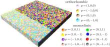
The ferroelectricity in BIT is simulated for both the monoclinic and the orthorhombic ferroelectric phases. The presence of these phases is inferred from the x-ray diffraction patterns of the BIT thin films experimentally grown via radio-frequency (RF) magnetron sputtering.[16] Different percentages of these orthorhombic (%VO and monoclinic (%VM phases are proposed for the simulations: {%VO, %VM} = {(50, 50), (60, 40), (70, 30), (80, 20), (40, 60), (30, 70), (20, 80)}. Each phase is uniformly distributed so as not to allow the random mixing of the dipole phases. The sample has a thin-film geometry with dimensions L × L × d, where L = 60 lattice units and d = 5 lattice units. An electric dipole with a unit magnitude is assigned to each lattice site. The spatial distribution of the dipoles has 12 possible directions: 8 in the monoclinic structure[21] and 4 in the orthorhombic symmetry, arising from the a(b)– c[22] and a(b) crystallographic axes, respectively. The initial assigned phase (orthorhombic or monoclinic) is preserved throughout the entire simulation, with no change in the electric field effect nor in the stress effect. Figure 1 shows the electric dipole distribution in the sample for monoclinic and orthorhombic fractions of 30 (%VO and 70 (%VM), respectively; each color represents an orientation of the electric dipole. For the simulation, the pinned dipole defects, which are induced in the presence of oxygen vacancies in the monoclinic or orthorhombic cell, are considered to occur in the direction of the applied electric field along the z axis, with positive and negative dipoles distributed randomly in percentages of 1%, 2%, 3%, 4%, and 5% in the monoclinic phase.
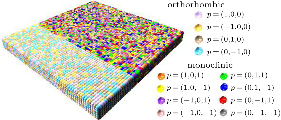 | Fig. 1. Distribution of electric dipoles in thin-film sample simulated with 70% (VM) monoclinic and 30% (Vo) orthorhombic phases and different orientations introduced. The sample has dimensions L × L × d with L = 60 lattice units and d = 5 lattice units. |
The Diffour Hamiltonian previously described by Laosiritaworn et al.[9] is employed for the average calculations of the hysteresis loops, which include the calculation of the stress as the ratio of the mechanical pressure to Young’ s modulus. The Hamiltonian reads[8]
 |
where 
 |
 |
where ε is Poisson’ s ratio, U0 is the ferroelectric interaction factor, P is the mechanical pressure, and Y is the Young’ s modulus. The reduced units are employed in the simulations. The ferroelectric interaction U0 is set to be 1, Ui j and E are in units of U0, and
 |
where N is the total number of electric dipoles in the lattice. A total of 5000 cycles are carried out to acquire the averaged hysteresis loops.
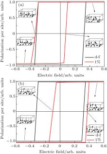
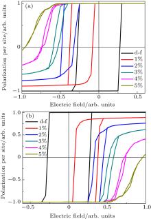
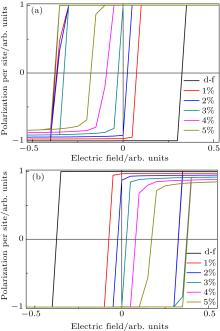
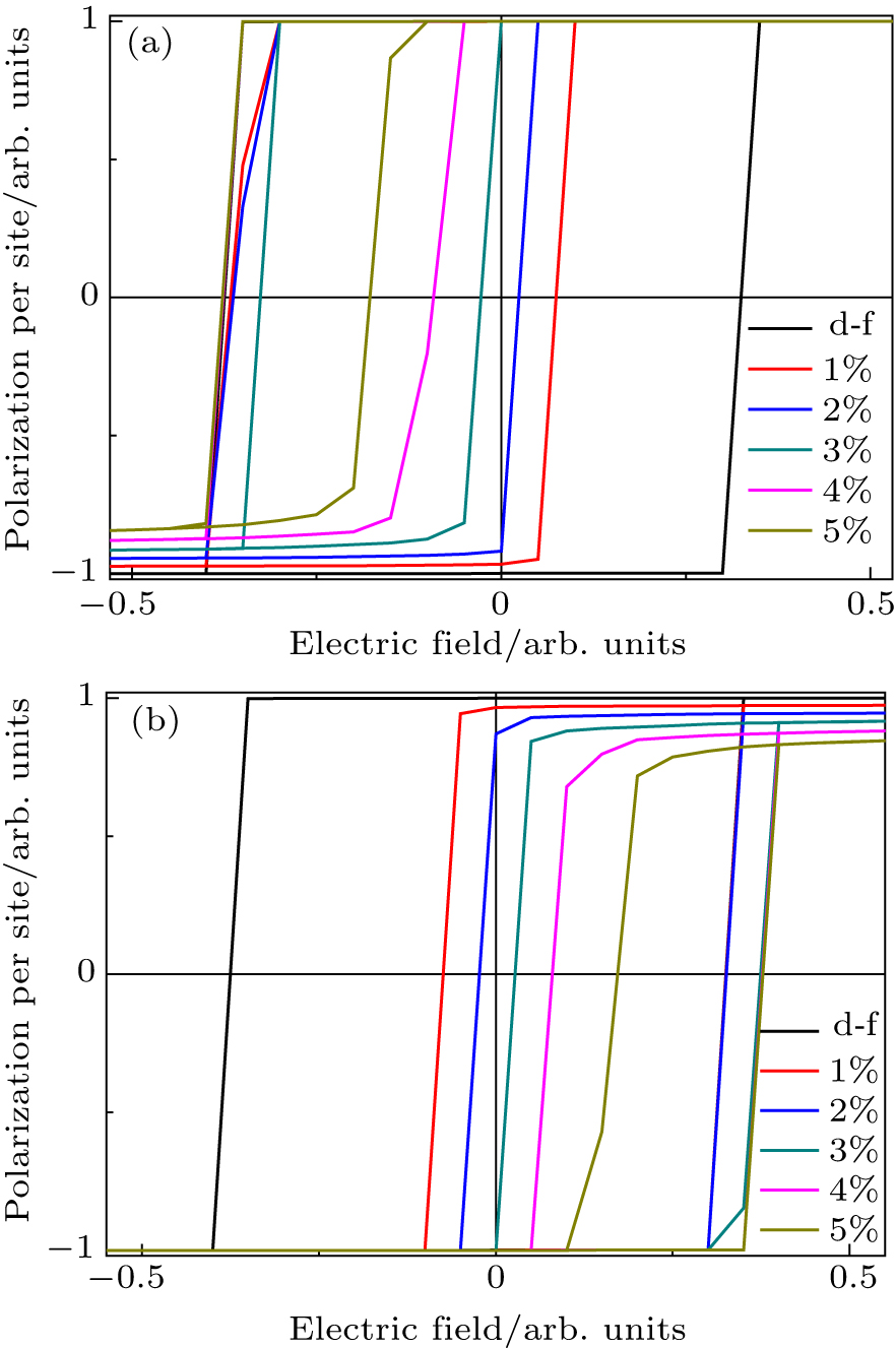
Figures 2– 4 show the simulated hysteresis loops for the monoclinic and orthorhombic phases, in defect-free (d-f) and pinned dipole defect samples, oriented in both the positive and negative z axes in various fractions. Well-defined and rectangular hysteresis loops are observed in the defect-free samples for all of the monoclinic and orthorhombic fractions. These loops can be obtained when the BIT samples are doped with Nb, [8] W, [24] La, [25] and others by reducing the concentration of oxygen vacancies, and also by the enhancement of the grain size. These ideal hysteresis loops tend to change when the defects are considered. For this case, it is difficult to obtain high-symmetry hysteresis loops because the dipolar defects caused by the oxygen vacancies tend to accumulate at the domain grain boundaries, leading to strong pinning of the domain walls; this is the major cause of degradation in the ferroelectric properties, [26, 27] hence affecting the measured remnant polarization Pr and coercive field Ec.[28] Since the electric field is applied in the z direction only, the monoclinic phase is sensitive to change (the orthorhombic phase has no component in this axis). This is illustrated in Fig. 2 for the sample with pinned dipoles of 1%, where the directions of dipoles in the monoclinic and orthorhombic phases can be observed. Consequently, as the orthorhombic fraction increases (Fig. 3), the hysteresis area diminishes. On the other hand, as the monoclinic fraction increases (Fig. 4), the hysteresis area increases, which can be attributed to a major population of non-pinned dipoles aligned with the electric field. Moreover, all the hysteresis loops (Figs. 2– 4) show an asymmetric trend. This asymmetry is reflected in the shift along the electric field axis, which is induced by the pinned dipole content. This phenomenon represents an imprint failure, which may be ascribed to an internal bias field that has been assigned to trapped charge carriers[29] or to a large internal stress induced by oxygen loss, [30] creating a preference for a certain polarization state. The extent of imprint in the sample is estimated by the shift in the mean coercive field as follows:[17]
 |
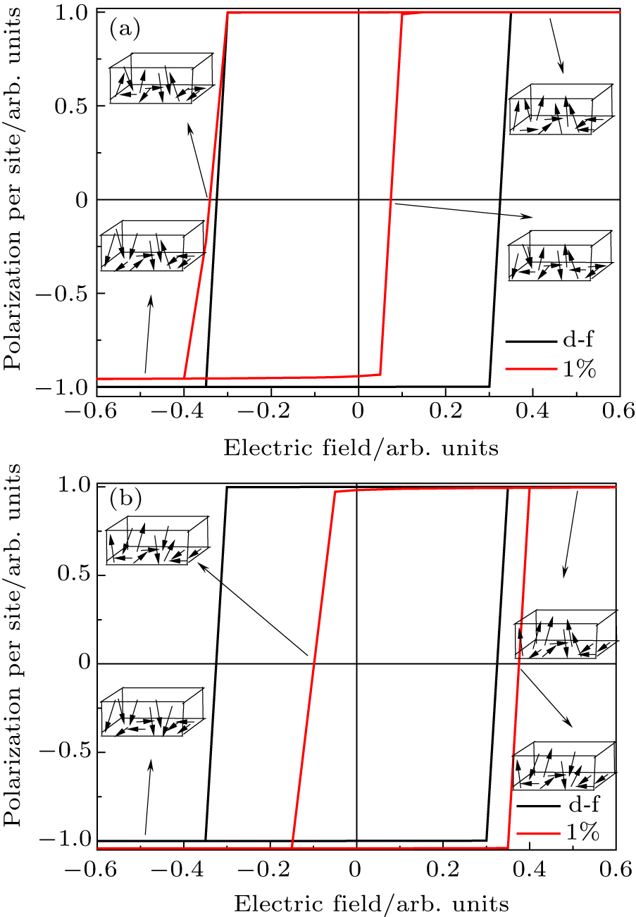 | Fig. 2. Hysteresis loops for 50% orthorhombic and 50% monoclinic phases, with defect-free (d-f) and dipole fraction of 1% pinned along the (a) positive and (b) negative z axis. |
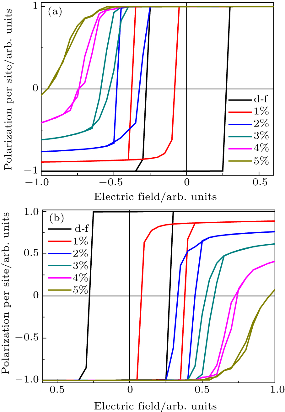 | Fig. 3. Hysteresis loops for 80% orthorhombic and 20% monoclinic phases, with various dipole fractions pinned along the (a) positive and (b) negative z axis. |
 | Fig. 4. Hysteresis loops for 20% orthorhombic and 80% monoclinic phases, with various dipole fractions pinned along the (a) positive and (b) negative z axis. |
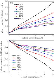
Figure 5 shows that the mean coercive field behaves as a function of the pinned dipoles oriented in the − z and + z directions for various monoclinic fractions. The increase in the pinned dipole fraction yields a higher mean coercive field because the defects force the defect-free dipoles to adopt a certain orientation (preventing them from switching back), as reported by Schorn et al.[17] The slopes in these curves depend on the pinned dipole orientation and the monoclinic phase fraction. A small concentration of the monoclinic phase leads to a major change in the mean coercive field, with the slope increasing, which can be explained by the larger imprint effects as shown in Fig. 3. The simulation of the imprint effect on ferroelectrics through the Monte Carlo method is attained by locating pinned dipoles in the direction of the electric field.
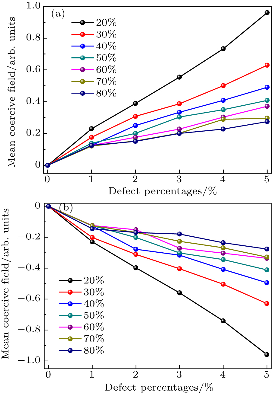 | Fig. 5. Variations of mean coercive field for monoclinic phases ranging from 20% to 80% with various dipole fractions pinned along the (a) negative and (b) positive z axis. |
When the pinned dipoles are positively oriented, the z axis offers easier polarization along this direction; as the concentration of the pinned dipoles increases, the strength of the electric field required to switch the dipoles to a negative orientation also increases (see Figs. 2– 4). When the sample is polarized in the negative z direction, the dipoles switch to a positive orientation with a smaller change in the electric field due to the decrease of the pinned dipole population along the negative axis with the increase in the concentration of the pinned dipoles. The polarization reduction in the direction opposite to the orientation of the pinned dipoles indicates that the number of dipoles participating in this switching process also decreases. A comparable shifting behavior is observed for pinned dipoles oriented along the negative z axis.
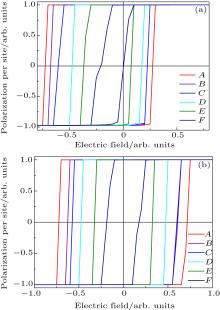
Figure 6 shows the hysteresis curves obtained for P/Y ratios, ranging from 0.06 to 0.11 in samples with 1% pinned dipoles in the + z direction and with defect-free dipoles. The shifts in the pinned dipole curves and a reduction in the hysteresis loop area with the increase of the mechanical stress are shown in Fig. 6(a). This reduction is remarkably lower than that observed in the defect-free samples (Fig. 6(b)). The stress has a notable effect on the shape of the curve. Since the stress is applied in the z direction, the axis becomes a hard axis; thus the decrease in the hysteresis area can be attributed to dipoles with out-of-plane components aligned in an anti-parallel manner in order to lower their energy. These results are consistent with those reported by Laosiritaworn et al., [8] in which the decrease in the hysteresis loop area due to the stress along the z axis of the free dipole sample was also explained by the preferential alignment of dipoles along the in-plane direction. Some experimental reports on the effect of the mechanical stress on the leakage current pointed out that such a reorientation process of domains under stress could reduce the density of the domain walls, which is known to play an important role in conducting, and so it may facilitate the suppression of the leakage current.[31]
 | Fig. 6. Hysteresis loops as a function of mechanical stress (P/Y): A = 0.06, B = 0.07, C = 0.08, D = 0.09, E = 0.10, F = 0.11, for (a) a sample containing 20% VO and 80% VM with pinned electric dipoles in the + z direction (1%) and (b) a defect-free sample. |
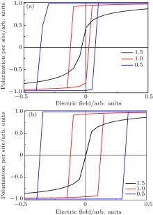
Finally, the effects of temperature (0.5U0/kB, 1U0/kB, and 1.5U0/kB) on the hysteresis loops of defect-free samples, as well as on samples featuring 1% of the dipoles pinned in the + z direction, are shown in Fig. 7. The narrowing of the hysteresis loops is observed at high temperatures, indicating a change from a ferroelectric state to a paraelectric state. In the pinned dipole samples (Fig. 7(a)), the shift along the field axis is related to the imprint effect; the abrupt diminution in the hysteresis area relative to the defect-free samples (Fig. 7b) is evidence of a loss of ferroelectricity. This can be explained as a decrease in the coercive field as temperature rises, bringing the sample to near the paraelectric state.[32]
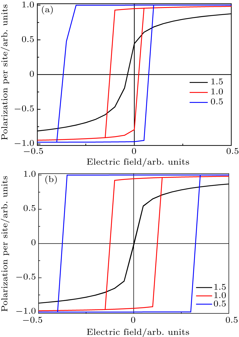 | Fig. 7. Hysteresis loops as a function of temperature for P/Y = 0.1 in (a) a sample containing 20% VO and 80% VM with pinned electric dipoles (1%) and (b) a defect-free sample. |
A ferroelectric study of Bi4Ti3O12 thin films is conducted via a Monte Carlo simulation of hysteresis loops to assess the presence of pinned dipoles and the effects of stress and temperature. The ferroelectric samples contain both monoclinic and orthorhombic phases and defects of pinned dipoles in various fractions. It is observed that the presence of the pinned dipoles vertically and horizontally shifts the hysteresis loops with the increase of the fractions of the pinned dipoles and the monoclinic phase. This effect can lead to an imprint failure mechanism that can cause degradation problems in ferroelectric materials. All of the findings in the present study reveal a ferroelectric interaction between the defects and the dipoles, in general agreement with both the experiment and the typical behavior expected in thin films with defects. The hysteresis loop area changes with the variation in the ratio of pressure to Young’ s modulus and with the temperature, which has been confirmed in other reports.
| 1 |
|
| 2 |
|
| 3 |
|
| 4 |
|
| 5 |
|
| 6 |
|
| 7 |
|
| 8 |
|
| 9 |
|
| 10 |
|
| 11 |
|
| 12 |
|
| 13 |
|
| 14 |
|
| 15 |
|
| 16 |
|
| 17 |
|
| 18 |
|
| 19 |
|
| 20 |
|
| 21 |
|
| 22 |
|
| 23 |
|
| 24 |
|
| 25 |
|
| 26 |
|
| 27 |
|
| 28 |
|
| 29 |
|
| 30 |
|
| 31 |
|
| 32 |
|