

Nanoscale domain switching mechanism of Bi3.15Eu0.85Ti3O12 thin film under the different mechanical forces
[Zhu Zhe†a)  , Chen Yu-Bo
a) , Zheng Xue-Junb) ]
, Chen Yu-Bo|
|


†Corresponding author. E-mail: akzhuzhe@126.com
*Project supported by the National Natural Science Foundation of China (Grant Nos. 51272158 and 11302185), the Scientific Research Fund of Hunan Provincial Education Department, China (Grant No. 13C901), and the Hunan Provincial Natural Science Foundation, China (Grant Nos. 14JJ3081 and 13JJ1019).
The switching process of ferroelectric thin films in electronic devices is one of the most important requirements for their application. Especially for the different external fields acting on the film surface, the mechanism of domain switching is more complicated. Here we observe the nanoscale domain switchings of Bi3.15Eu0.85Ti3O12 thin film under different mechanical forces at a fast scan rate. As the force increases from initial state to 247.5 nN, the original bright or grey contrasts within the selected grains are all changed into dark contrasts corresponding to the polarization vectors reversed from the up state to the down state, except for the clusters. As the mechanical force increases to 495 nN, the color contrasts in all of the selected grains further turn into grey contrasts and some are even changed into grey contrasts completely showing the typical 90° domain switching. When another stronger loading force 742.5 nN is applied, the phase image becomes unclear and it indicates that the piezoelectric signal can be suppressed under a sufficiently high force, which is coincident with previous experimental results. Furthermore, we adopt the domain switching criterion from the perspective of equilibrium state free energy of ferroelectric nanodomain to explain the mechanisms of force-generated domain switchings.
In the smart sensor and actuator applications for active vibration suppression, ferroelectric thin film is subjected to cyclic stress and electric field loading, which can cause device degradation. The intrinsic material property makes ferroelectric thin film useful as sensors and actuators.[1, 2] One of the most important requirements for ferroelectric thin films in electronic devices is the switching process between two opposite polarization states. The ability to change the direction of polarization by using an applied electric field or stress can lead to the motion of the domain wall and domain switching evolution.[3, 4] The stress and electric field levels sufficient to cause ferroelectric thin film domain switching are relatively low and the device designer must understand them. Lead-free ferroelectric thin film materials for micro-electro-mechanical system (MEMS) applications are desirable on environmental grounds as well as for biocompatibility. Previous studies in recent years have revealed that Bi3+ ions in the Bi4Ti3O12 structure could be substituted by trivalent rare earth ions in order to improve the ferroelectric properties.[5– 8] Bismuth titanate-based thin films, which are comparable to conventional lead-based ferroelectric thin films, have therefore been considered to be candidates for sensor and actuator applications.
There are many papers about the electric-generated domain switching by piezoresponse force microscopy (PFM), [9, 10] but few studies focusing on the effect of mechanical stress are reported. Balke et al. discovered the effect of dragging a PFM tip on the switching response of ferroelectrics, [11] and Bea et al. explained it in terms of the ferroelastic coupling inherent in these ferroelectrics.[12] Alguero et al. pointed out the stress-induced suppression of the piezoelectric coefficient.[13] The flexoelectric effect which permits the switching of devices in nonpolar (non-piezoelectric) crystals by using inhomogeneous stresses is receiving increasing attention.[14, 15] However, research about the force-generated domain switching process is not comprehensive enough and the mechanism of polarization reverse under mechanical force is not very clear. Therefore, we experimentally observe the polarization reverse processes of Bi3.15Eu0.85Ti3O12 (BET) thin film under different mechanical forces, and the simultaneous piezo-phase images of the domain switching evolution are recorded to understand the mechanism of force-generated domain switching.
BET thin film with a thickness of 300 nm was deposited on Pt/TiO2/SiO2/Si (111) substrate by metal-organic decomposition (MOD) and annealed at 700 ° C in an oxygen atmosphere. The preparation was described in our previous study.[16] The crystal structure of BET thin film was investigated by x-Ray diffraction (XRD) (X’ Pert Pro, Holland) patterns through scanning at 4° /min with Cu Kα radiation (40 kV, 10 mA). The circular Au top electrodes with a radius of 0.1 mm were deposited on the films using a shadow mask by dc magnetron sputtering, and the Au/BET/Pt capacitors were obtained. The polarization– electric field (P– E) hysteresis loop under a bipolar driving field of 400 kV/cm was measured at 1 kHz by a ferroelectric tester (Radiant Technologies, Precision Workstation, USA).
PFM with a diamond coated cantilever (with a tip apex radius of 40 nm, a spring constant of 3 N/m, Veeco) was used to characterize the piezoelectric property and carry out the domain switching under a resonance frequency of approximately 300 kHz. The measurement was performed by keeping the PFM tip fixed above the grain and applying a dc voltage from − 10 V to 10 V when recording the piezoelectric signal. Considering the local method of piezoelectric characterization for PFM, the piezoelectric measurement was repeatedly conducted on 10 points within the scanned scope of the sample surface. During the domain switching, after applying force to the thin film, an ac signal Vac = V0 sin (ω t) with an amplitude of 1 V and a frequency of 60 kHz was applied between the PFM tip (movable top electrode) and sample bottom electrode to acquire domain images. Switching implies permanent change between two metastable configurations. So the obtained phase images were all measured under identical conditions. The PFM setpoint was stepped in order to vary the mechanical forces exerted by the tip on the thin film surface. It should only be mentioned that our experimental conditions (appropriate spring constant of 3 N/m with the sharp tip and stiff cantilever) corresponded to a so-called “ strong indentation” regime where the measured signal was mainly due to the piezoelectric vibration of the surface and not the electrostatic contribution.[17] The increasing mechanical forces were exerted on the film surface of 750 nm× 750 nm and the induced piezo-phase images were observed to understand the domain evolution, including nucleation, coalescence and growth. Note that, although the loading force was ∼ 1000 nN, with a corresponding local stress of 3 GPa (approximating the tip-surface contact area as a disk of 10 nm in radius), it was still well below the threshold (∼ 20 GPa) for irreversible plastic damage of the thin film surface.[18]
The XRD pattern confirms that the BET thin film shows typical XRD patterns of the Bi-layered perovskite polycrystalline structure and random orientation without pyrochlore phase, as shown in Fig. 1(a). The inset displays a polarization-electric field hysteresis loop of BET thin film, and 2Pr value is 84 μ C/cm2, which is comparable to that of Bi3.25Eu0.75Ti3O12 thin film: 66 μ C/cm2 in previous study and benefits polarization switching. The typical D– V curve and d33– V loop of BET thin film are given in Fig. 1(b). On the D– V curve, there is no notable horizontal shift, and a small vertical shift (0.04 nm) can be observed, indicating no obvious imprint effect. According to 10 piezoelectric measurements, the average d33 value of BET thin film is 39.6 pm/V. The d33– V loop clearly shows that the BET thin film is switchable and the piezoelectric is retained.[19]
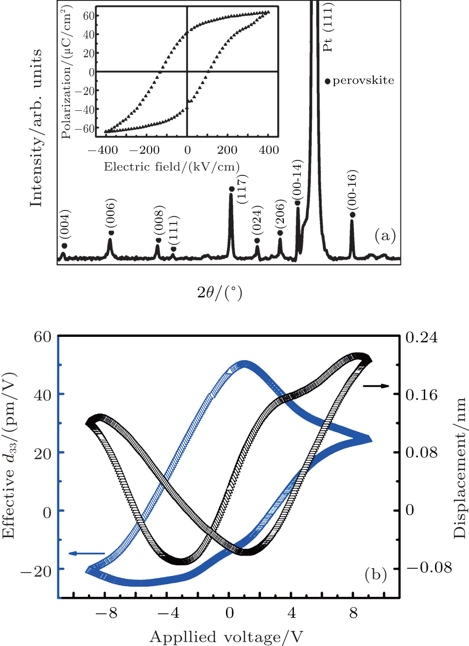 | Fig. 1. The XRD pattern with the inset of topography image (a), the typical D– V curve and d33– V loop of BET thin film (b). |
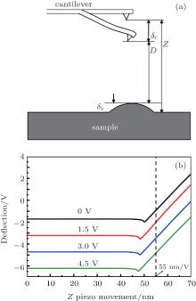
Unlike the situation with applying an electrical field, the real forces from the PFM tip are obtained through data conversion. The different forces applied to thin film correspond to the parameters of cantilever deflection setpoints Uc: 0.01 V, 1.5 V, 3 V, and 4.5 V. Figure 2(a) shows the relationship between the tip-sample distance and cantilever amplitude and figure 2(b) shows the plots of cantilever deflection dc versus sample position along the z axis. The cantilever sensitivity Δ is determined from the slope of the force-plot curve and equals 55 nm/V. The cantilever deflection δ c can be derived from δ c = Δ × Uc. A simple relationship (i.e. Hooke’ s Law) between the force F and the cantilever deflection is F = − k· δ c, where k is the spring constant of the cantilever and equals 3 N/m in our experiment. According to the above calculation results, we know that the forces at the cantilever deflection setpoints of 0.01 V, 1.5 V, 3 V, and 4.5 V are 1.65, 247.5, 495, and 742.5 nN. Meantime, the PFM tip will work at a fast scan rate of 1.2 Hz.
 | Fig. 2. Schematic diagram of the relationship between the tip-sample distance and cantilever amplitude (a), and plots of cantilever deflection dc as versus sample position along the z axis under the dc deflection setpoints of 0 V, 1.5 V, 3 V, and 4.5 V (b). |
Typical topography maps of an area of 750 nm× 750 nm and simultaneously piezoelectric phase images of BET thin film are obtained at 1.65, 247.5, 495, and 742.5 nN, respectively, as shown in Figs. 3(a)– 3(h). In Figs. 3(a) and 3(b) at 1.65 nN, there are clear grain boundaries, and a few pinholes and voids on the film surface. The crack-free structure is good for the microstructure and ferroelectric properties.[20] The grain size approximately ranges from 50 nm to 150 nm. In order to describe the domain evolution more clearly, we carry out statistical treatment and choose ten single grains and other two clusters with multiple grains to observe the domain switchings within them. The selected single grains and clusters are numbered from 1 to 12 and are marked by loops in topography images and phase images. For the phase image in Fig. 3(b), we draw the arrows to denote three typical color contrasts: pure white (W), black (B), and grey (G), moreover the multicolor contrasts are also observed. Generally, domains with different polarities exhibit different contrasts in piezoelectric phase image.[21] The dark region corresponds to c+ -domains with polarization terminated at the free surface of the film, the bright region corresponds to c− -domains polarization with orientation towards the bottom electrode, the gray areas represent in-plane polarization and the multicolor regions to the polarization vector at some angle with respect to film’ s plane. For the selected single grains and clusters in Fig. 3(b), we can summarize three types of domain configurations: those which appear mainly to be bright and are marked by black loops in grains 2– 4, those which appear mainly to be dark and are marked by white loops in grains and clusters 6– 12, and those which appear mainly to be grey and are marked by blue loops in grains 1 and 5. We will study the domain switchings under mechanical forces in accordance with the three kinds of them. As the mechanical force increases to 247.5 nN shown in Figs. 3(c) and 3(d), the surface morphology in Fig. 3(b) has some change. The original bright contrasts within grains 2– 4 are all changed into partially dark contrasts corresponding to 180° -domain switching. The original bright or grey color areas within grains and clusters 6– 12 in Fig. 3(b) also tend to be dark, except for clusters 9 and 12. We notice that the clusters 9 and 12 are all composed of several small grains and the formed grain boundary potential barriers in these cluster may impede the domain-wall movement each other, leading to irregular domain reverse.[22] The original grey contrasts in grains 1 and 5 become partially dark, which shows a similar result. In our previous paper, [23] the domain evolution at lower force with a slow scan rate of ∼ 0.1 Hz, shows the typical 90° domain switching in the whole process. The phase image in Fig. 3(d), by contrast, seems to be an unexpected result. Note that the grains can be dragged and have some deformations, especially at a fast scan rate with the force increasing from initial state to 247.5 nN and the compressive force is weakened. So the non 90° domain switching is observed. Then with the mechanical force increasing to 495 nN shown in Figs. 3(e) and 3(f), the grains are still smooth and crack-free and the color contrasts in all selected grains turn into grey contrasts compared with the initial states. Some of them are even changed into grey contrasts completely, as shown in grains 2– 4. This means that the polarization vectors are reversed from a perpendicular to a parallel direction; namely, 90° domain switching occurs after increasing the loading forces. This happens because the compressive force becomes dominated when the loading force increases to 495 nN further. In Figs. 3(g) and 3(h), another stronger loading force 742.5 nN is then applied and there is no one-to-one correlation between topography and piezoelectric image, which reflects that the weak piezoelectric signal is created. It is suggested that the piezoelectric signal can be suppressed under sufficiently high force, which is coincident with the previous experimental result.[24] Lu et al.[25] also pointed out that the amplitude decreases as load increases and the threshold is at an applied force of ∼ 750 nN, which is close to the loading force 742.5 nN.
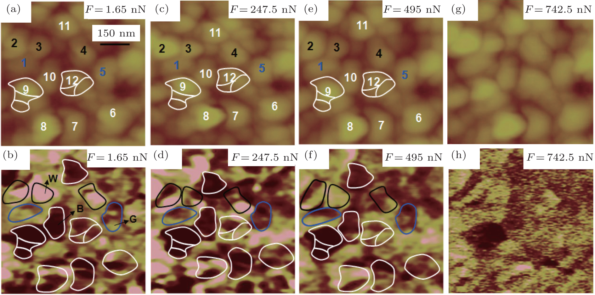 | Fig. 3. Topography images and simultaneous PFM phase images taken at different mechanical forces: 1.65 nN ((a) and (b)), 247.5 nN ((c) and (d)), 495 nN ((e) and (f)), and 742.5 nN ((g) and (h)). |
In order to explain the domain switching mechanism more clearly, we adopt the domain switching criterion which comes from the perspective of equilibrium state free energy and has been used to explain the domain switching mechanism under the electric field.[26] Based on this concept, it is assumed that the crystal is in a stable state at any time and the dynamics of the switching process itself or any hysteresis effect is not taken into consideration. For one single grain, the driving force for kinds of domain switchings can be determined by[26]

where Δ G, Ps, E3, d33, and σ 3 are the difference in Gibbs energy of domain between the initial state and the state after switching, the spontaneous polarization, external electric field, effective piezoelectric coefficient, and compressive stress, respectively. If the difference Δ G is less than zero, then the electric field generated nanoscale domain switching will be dominated, corresponding to 180° domain switching. While the difference Δ G is greater than zero, the electric field generated domain switching will be weakened and force-generated domain switching will be dominated, corresponding to 90° -domain switching.
Generally, E3 (E3 > 0) is from the testing voltage and is very small, and σ 3 (σ 3 < 0) is from compressive loading force. Therefore, the existence of second term on the right-hand in Eq. (1) opposes the first one if PS is positive (d33 is positive by definition). With the increase of loading force at a slow scan rate, the difference Δ G will be larger than zero, corresponding to the typical 90° -domain switching. However, in contrast from the condition at a slow scan rate, the compressive loading force at a fast scan rate will generate a horizontally shearing (lateral) force, which cannot be neglected in Δ G. The shearing stress induced by the PFM tip, namely the nonzero σ xx components would tend to prefer local a domains (in plane polarization component). So the term − ε s · σ xx will be added into Eq. (1), which can be expressed as

where ε s is the induced strain. At the beginning, when mechanical force increases from initial state to 247.5 nN, the negative term − ε s · σ xx opposes the difference Δ G in Eq. (1) and the difference Δ G in Eq. (2) is close to a negative value, corresponding to the 180° -domain switching, as shown in Fig. 3(d). With the increase of mechanical force, the absolute value of σ 3 gradually increases, the difference Δ G in Eq. (2) will be close to a positive value, corresponding to the 90° domain switching, as shown in Fig. 3(f).
The nanoscale domain switchings of BET thin film are observed by piezoresponse force microscopy under different mechanical forces during the fast scan. As the mechanical force increases from initial state to 247.5 nN, the original bright contrasts within grains 2– 4 are all changed into contrasts. The original bright or grey color contrasts within grains and clusters 6– 12 are changed into grey, except for clusters 9 and 12. Meanwhile, the original grey contrasts in grains 1 and 5 become partially dark. As the mechanical force increases to 495 nN, the color contrasts in all of the selected grains are further faded. Some are even changed into grey contrasts, which are completely shown in grains 2– 4. This means that 90° -domain switching occurs after the loading forces have been increased. Moreover, when another stronger loading force of 742.5 nN is applied, the piezoelectric signal can be suppressed under a sufficiently high force, which is coincident with the previous experimental results. The mechanisms of force-generated nanoscale domain switchings at different scan rates are explained uniformly by the domain switching criterion from the perspective of equilibrium state free energy. The difference between two domain states Δ G including the stress term can be considered as a switching criterion defined by the different values of Δ G. These results will provide an additional insight into the estimate of the working limit parameter on stress sensors.
| 1 |
|
| 2 |
|
| 3 |
|
| 4 |
|
| 5 |
|
| 6 |
|
| 7 |
|
| 8 |
|
| 9 |
|
| 10 |
|
| 11 |
|
| 12 |
|
| 13 |
|
| 14 |
|
| 15 |
|
| 16 |
|
| 17 |
|
| 18 |
|
| 19 |
|
| 20 |
|
| 21 |
|
| 22 |
|
| 23 |
|
| 24 |
|
| 25 |
|
| 26 |
|