Low insertion loss silicon-based spatial light modulator with high reflective materials outside Fabry–Perot cavity
Tian Li-Fei1, 2, Kuang Ying-Xin1, 2, Fan Zhong-Chao2, †, Li Zhi-Yong1, ‡
State Key Laboratory on Integrated Optoelectronics, Institute of Semiconductors, Chinese Academy of Sciences, Beijing 100083, China
Engineering Research Center for Semiconductor Integrated Technology, Institute of Semiconductors, Chinese Academy of Sciences, Beijing 100083, China


† Corresponding author. E-mail: zcfan@semi.ac.cn lizhy@semi.ac.cn

Project supported by the National Natural Science Foundation of China (Grant Nos. 61575076 and 61804148) and the National Key Research and Development Plan of China (Grant No. 2016YFB0402502).

Abstract

The extinction ratio and insertion loss of spatial light modulator are subject to the material problem, thus limiting its applications. One reflection-type silicon-based spatial light modulator with high reflective materials outside the Fabry–Perot cavity is demonstrated in this paper. The reflectivity values of the outside-cavity materials with different film layer numbers are simulated. The reflectivity values of 6-pair Ta2O5/SiO2 films at 1550 nm are experimentally verified to be as high as 99.9%. The surfaces of 6-pair Ta2O5/SiO2 films are smooth: their root-mean-square roughness values are as small as 0.53 nm. The insertion loss of the device at 1550 nm is only 1.2 dB. The high extinction ratio of the device at 1550 nm and 11 V is achieved to be 29.7 dB. The spatial light modulator has a high extinction ratio and low insertion loss for applications.

1. Introduction

Spatial light modulators play a significant role in application fields of space optical communication, optical calculation, biochemical sensing and digital holography imaging.[17] With the rapid development of information era, spatial light modulators are expected to promote the performance improvement of products including unmanned aerial vehicles, micro-satellites, and optical broadband networks.[813] Spatial light modulators can modulate the light intensity, phase, and polarization.[1418] Spatial light modulators can be divided into reflective and transmissive modes according to the different ways of reading out light. Compared with the transmission type, the reflection-type spatial light modulator is a new device with high resolution, contrast, pixel opening rate, and energy utilization efficiency.[1923] The optical structure of silicon-based spatial light modulator contains a Fabry–Perot (FP) cavity, Mach–Zehnder interferometer, Bragg optical grating, and micro-ring resonant cavity.[2431] The silicon-based spatial light modulators can be fabricated through a mature microelectronic fabrication technology called complementary metal–oxide–semiconductor process which has low cost, high integration, and high processing precision. However, the extinction ratio of the present spatial light modulator is low and the insertion loss is high for practical applications due to materials problems.[3237]

Here in this work, we propose a reflection-type silicon-based spatial light modulator with Fabry–Perot cavity structure. We adopt the dielectric thin film to replace the traditional metal film in order to reduce the insertion loss.[33] At the same time, we use the polycrystalline silicon (poly-Si) film as an inside-cavity layer to obtain longer service life than the previous polymer material. The reflectivity values of the outside-cavity materials with different film layer numbers are simulated. The reflectivity, refractivity, surface, and cross-section morphologies, and surface roughness values of the outside-cavity materials are measured. The effect of driving voltage on reflectivity of the spatial light modulator is investigated to gain the extinction ratio and insertion loss.

2. Device design and simulation

Figure 1(a) demonstrates the schematic diagram of designed cross-sectional spatial light modulator unit with FP cavity. The materials outside the cavity, i.e., 6-pair Ta2O5/SiO2 thin films constitute the reflecting mirror. The material inside the cavity, i.e., poly-Si film, is used as an isolation layer. The heating electrode on the surface of isolation layer is of Au/Ti. The substrate is of monocrystalline silicon. Figure 1(b) displays the heating electrode on the surface of isolation layer. The device contains a 50 × 5 array with single pixel size of 0.2 mm ×2 mm.

Fig. 1. Schematic diagram of designed spatial light modulator unit with FP cavity: (a) schematic diagram of cross section and (b) schematic diagram of heating electrode on surface of isolation layer.

The reflectivity spectra of the outside-cavity materials with different film layer numbers are simulated according to transfer matrix method (TMM)[38] in order to obtain the optimal values. The simulation architecture includes the silicon substrate, the Ta2O5/SiO2 multilayer films, and the air. The reflectivity of outside-cavity material R can be expressed as follows: where is the effective refractivity of the incident medium, i.e., air; B and C are characteristic matrix elements of Ta2O5/SiO2 multilayer film, which can be calculated from the following formula: where k is the layer number of Ta2O5/SiO2 multilayer films, is the phase thickness of the j-layer film, is the effective refractivity of the j-layer film, is the effective refractivity of the last layer film, i.e., substrate, and i is the imaginary factor.

The value of can be calculated from the following equation on condition that the incident angle is zero: where nj is the refractivity of the j-layer film, dj the vertical thickness of the j -layer film, and λ the wavelength of the incident light. The effective refractivity of the film is equal to the refractivity as the incident angle is zero.

Figure 2(a) exhibits the simulation curves of the reflectivity of the outside-cavity material R versus the wavelength of the incident light for the film layer odd number k from 1 to 15. The SiO2 and Ta2O5 films are arranged alternatively. The first layer is SiO2 film with low refractivity, the second layer is Ta2O5 film with high refractivity, and so on. The reflectivity of the outside-cavity material at 1550 nm can exceed 91.4% as the odd number of outside-cavity material is not less than 11.

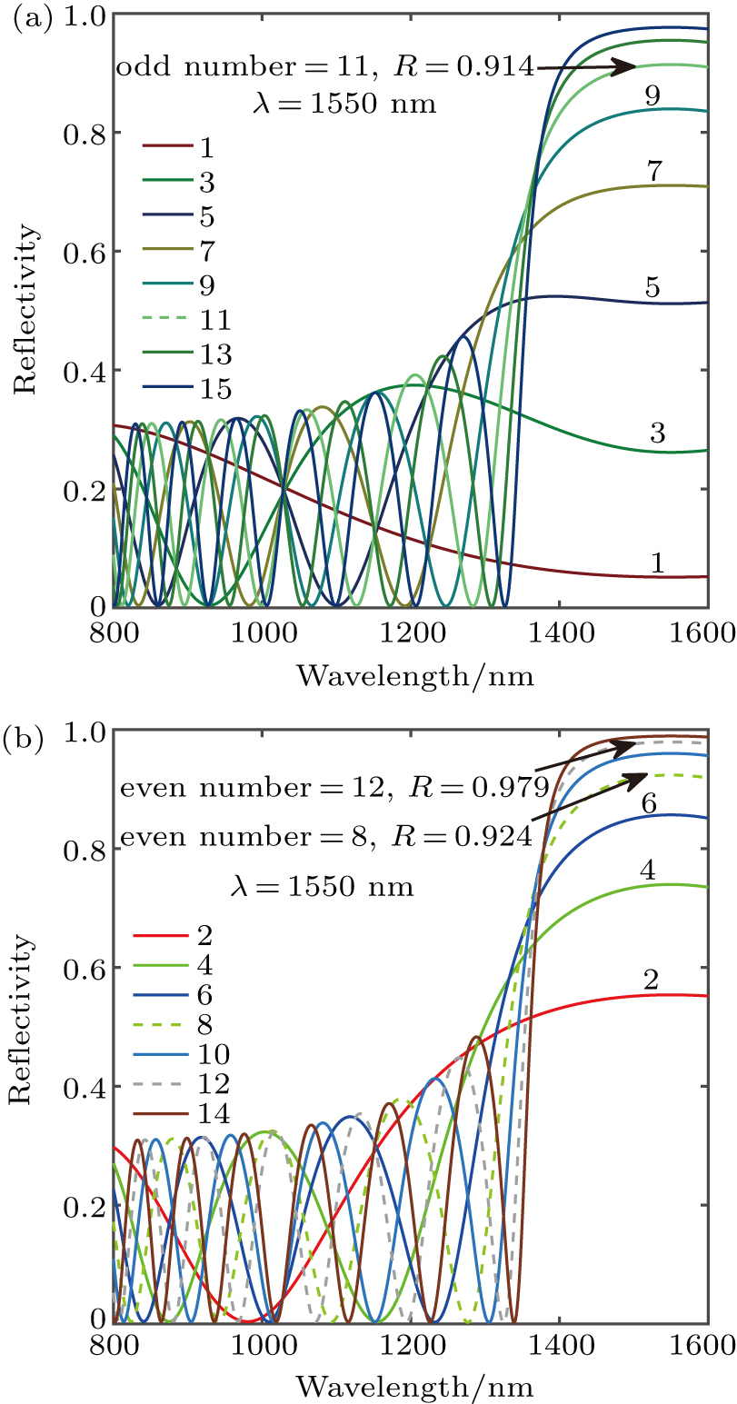
Fig. 2. Simulation curves of reflectivity of outside-cavity material R versus wavelength of incident light for film layer (a) odd number from 1 to 15 and (b) even number from 2 to 14.

Figure 2(b) shows the simulation curves of the reflectivity of outside-cavity material R versus the wavelength of incident light with the film layer even number k from 2 to 14. The reflectivity of outside-cavity material at 1550 nm can exceed 92.4% as the even number of the outside-cavity materials is not less than 8.

The even-number film layers are apparently better to realize high reflectivity than the adjacent odd-number film layers. The outside-cavity materials with even number of 12 are chosen to realize both low stress and high reflectivity (97.9%) at 1550 nm.

3. Experiment

The thin films of lower 6-pair Ta2O5/SiO2, poly-Si, and upper 6-pair Ta2O5/SiO2 were deposited on the a-plane silicon substrate orderly. The SiO2 and Ta2O5 thin films with thickness of 260 nm and 190 nm were deposited by ion beam sputtering process. The poly-Si film with a thickness of 100 nm was deposited by chemical vapor deposition. The electrode of Ti and Au films with thickness of 50 nm and 350 nm were deposited by electron beam evaporation. The pattern structures of upper 6-pair Ta2O5/SiO2 and electrode were fabricated by ultraviolet lithography and inductively coupled plasma etch technology, successively.

The refractivity values of the thin films were measured using ellipsometer (J A Woollam, M-2000DI). The surface and cross-section morphologies were analyzed by scanning electron microscopy (SEM, FEI, NanoSEM650). The surface roughness values of the thin films were gained by atomic force microscopy (AFM, Bruker, DimensionEdge). The reflectivity values of the outside-cavity materials with wavelength ranging from 800 nm to 1600 nm were analyzed by spectrophotometer (PerkinElmer, Lambda 1050). The incident light of the spatial light modulator was generated from a tunable laser (Yokogawa, AQ2200-136) and a fiber collimator. The reflectivity values of the spatial light modulator with wavelength ranging from 1550 nm to 1600 nm were obtained by optical spectrum analyzer (Yokogawa, AQ6370 C). The voltages exerted on spatial light modulator were introduced from a direct current power supply (Gwinstek, GPD3303 S).

4. Results and discussion

Figure 3(a) displays the variations of measured refractivity with wavelength of SiO2 and Ta2O5 thin film. With the increase of wavelength from 800 nm to 1600 nm, the refractivity value of SiO2 and Ta2O5 thin film both reduce gradually and slightly, neither of their decrements is more than 0.22. The refractivity values of SiO2 and Ta2O5 thin film at 1550 nm are 1.4847 and 2.0723, respectively.

Fig. 3. (a) Measured refractivity versus wavelength of SiO2 and Ta2O5 thin films, (b) simulated and measured reflectivity spectrums of 6-pair Ta2O5/SiO2 thin film.

Figure 3(b) shows the simulated and measured reflectivity spectrum of the 6-pair Ta2O5/SiO2 thin film. The simulated and measured reflectivity at 1550 nm are 97.9% and 99.9%, respectively. They are highly consistent with each other and the degree of disparity is solely 2%. The measured reflectivity at 1550 nm is slightly higher than the simulated reflectivity.

The surface and cross-section morphology, and surface roughness of the outside-cavity materials are measured to ascertain why the measured reflectivity is higher than simulated reflectivity.

Figure 4(a) shows the cross-section SEM image of the 6-pair Ta2O5/SiO2 thin films. The inset shows the surface SEM image of the thin films. The surface particle size of the 6-pair Ta2O5/SiO2 thin films is fine (less than 2 nm) and uniform. It indicates that the 6-pair Ta2O5/SiO2 thin films are extremely compact, which can reduce the bulk scattering loss of light and raise the reflectivity of films.[39]

Fig. 4. Morphologies and surface roughness of 6-pair Ta2O5/SiO2 thin films: (a) cross-section and surface (inset) SEM image, and (b) two-dimensional and three-dimensional (inset) AFM image.

Figure 4(b) demonstrates the two-dimensional and three-dimensional (inset) AFM image of the 6-pair Ta2O5/SiO2 thin films. The surface root-mean-square roughness (RMS) is small, only 0.53 nm. The surface roughness is not considered in the simulation method. The reflectivity including the influence of surface roughness is defined by the equation in the normal incident case[40,41] where Rr is the reflectivity of real film, Rp the reflectivity of film with perfectly smooth surface, σ the RMS of film, and λ the wavelength of incident light. The smaller the RMS of film, the lower the total integrated scattering of light is and the higher the reflectivity of real film Rr. The surface of the 6-pair Ta2O5/SiO2 thin films is comparatively smooth, which can lessen the surface scattering loss of light and enhance the reflectivity of films.

The reflectivity values of spatial light modulator at different voltages are investigated in order to calculate the extinction ratio and insertion loss. The extinction ratio ER is defined by the equation: where R0 is the reflectivity without voltage, and R1 is the reflectivity with voltage.

The insertion loss IL is expressed by the formula: where R0 is the reflectivity without voltage.

Figure 5(a) shows the reflectivity spectra of the spatial light modulator with the logarithmic vertical axis in a voltage range from 0 V to 6 V. The test point is in the center of a single pixel. The reflectivity values of device within the range from 1550 nm to 1600 nm are nearly constant as the voltage increases from 0 V to 6 V.

Fig. 5. Reflectivity spectra of spatial light modulator at voltages (a) from 0 V to 6 V, and (b) from 8 V to 11 V, and (c) at 1550 nm.

Figure 5(b) displays the reflectivity spectra of the spatial light modulator in a voltage range from 8 V to 11 V. The reflectivity values of device within the range from 1550 nm to 1600 nm present a degrading trend as the voltage rises from 8 V to 11 V.

Figure 5(c) exhibits the reflectivity values of the spatial light modulator at 1550 nm in a voltage range from 0 V to 11 V. The insertion loss of the spatial light modulator at 1550 nm is 1.2 dB. The low insertion loss is ascribed to the good quality dielectric films outside the FP cavity with high reflectivity. The extinction ratio of the spatial light modulator at 1550 nm at 11 V is 29.7 dB. It means that the modulation depth of the spatial light modulator at 1550 nm is as high as 99.9%.

The reflectivity of our spatial light modulator in the normal incident case RM can be calculated from the following formula[42] where R is the reflectivity of outside-cavity materials, n the refractivity of inside-cavity material, L the thickness of poly-Si film, λ the wavelength of incident light. The L is expressed as , where, is the resonance wavelength under the action of voltage, i.e., 1550 nm; is the refractivity of poly-Si film under the action of voltage. RM under the action of voltage is designed to be a minimum value. As the voltage change is identical, the bigger thermo-optic coefficient of poly-Si film can lead to the higher refractivity variation, and bring about the more obvious reflectivity variation of spatial light modulator, resulting in the higher extinction ratio. Therefore, the high extinction ratio of the spatial light modulator is due to the excellent thermo-optic effect[43] of poly-Si film inside the FP cavity. The critical voltage of 6 V appears because the thermo-optic effect of poly-Si film becomes remarkable at sufficiently high voltage.

5. Conclusions

In this work, we demonstrate a reflection-type silicon-based spatial light modulator with high reflective materials outside the Fabry–Perot cavity. The outside-cavity dielectric Ta2O5/SiO2 thin films present smooth surfaces. The spatial light modulator has high extinction ratio and low insertion loss at 1550 nm. The low insertion loss is ascribed to the good quality dielectric films with high reflectivity. The high extinction ratio is due to the excellent thermo-optic effect of poly-Si film. The modified materials can improve the performances of the device for applications.

Reference
[1] Feng F White I H Wilkinson T D 2013 J. Lightwave Technol. 31 2001
[2] Gailele L Dudley A Forbes A 2018 Conference on Laser Beam Shaping XVIII August 20–21, 2018 San Diego, USA 1074414 10.1117/12.2505725
[3] Mills B Thomson D J Mashanovich G Z Reed G T Vynck K Muskens O L Lalanne P Bruck R 2016 Optica 3 396
[4] Lutkenhaus J Lowell D George D Zhang H Lin Y Lin Y 2016 Micromachines 7 59
[5] Ni H Zou L Guo Q Ding X 2017 Opt. Express 25 2872
[6] Li L Xie G Ren Y Ahmed N Huang H Zhao Z Liao P Lavery M P Yan Y Bao C 2016 Appl. Opt. 55 2098
[7] Wang Y Ren Y Chen L Song C Li C Zhang C Xu D Yao J 2018 Chin. Phys. B 27 114204
[8] Du X Chang J Zhang Y Wang X Zhang B Gao L Xiao L 2015 Opt. Express 23 26032
[9] Ouyang B Hou W Caimi F M Dalgleish F R Vuorenkoski A K Gong S Britton W 2015 Conference on Compressive Sensing IV April 22–24, 2015 Baltimore, USA 94840I 10.1117/12.2178804
[10] Gutierrez F A Perry P Martin E P Ellis A D Smyth F Barry L P 2015 J. Lightwave Technol. 33 5073
[11] Mathis A Froehly L Toenger S Dias F Genty G Dudley J M 2015 Sci. Rep. 5 12822
[12] Sun S Zhang R Peng J Narayana V K Dalir H El-Ghazawi T Sorger V J 2018 Opt. Express 26 8252
[13] Xia X W Ewing T K Serati S A Fu Y J Zhou R Neff J A Barnes F S 2003 Conference on Active and Passive Optical Components for WDM Communications III August 14, 2003 Orlando, USA 95 10.1117/12.509153
[14] Wang H T Zhou D B Zhang R K Lu D Zhao L J Zhu H L Wang W Ji C 2015 Chin. Phys. Lett. 32 084203
[15] Zhou D B Wang H T Zhang R K Wang B J Bian J An X Lu D Zhao L J Zhu H L Ji C Wang W 2015 Chin. Phys. Lett. 32 054205
[16] Cao Y M Wu B J Wan F Qiu K 2018 Acta Phys. Sin. 67 094208 in Chinese
[17] Liu Y K Wang X L Su R T Ma P F Zhang H W Zhou P Si L 2017 Acta Phys. Sin. 66 234203 in Chinese
[18] Liu X Yang L Ma J Li C Jin W Bi W 2018 Chin. Phys. B 27 104206
[19] Imura T Koga H Lim P B Umezawa H Horimai H Inoue M 2006 Conference on Optical Information Systems IV August 16–17, 2006 San Diego, USA 631115 10.1117/12.680269
[20] Takizawa K Kikuchi H Fujikake H Okada M 1990 Appl. Phys. Lett. 56 999
[21] Pan R P Shieu C R Lu W L Huang M J Pan C L 2001 Conference on Spatial Light Modulators July 31–August 01, 2001 San Diego, USA 111 10.1117/12.447745
[22] Takahashi K Kawanishi F Mito S Takagi H Shin K H Kim J Lim P B Uchida H Inoue M 2008 J. Appl. Phys. 103 07B331
[23] Hwang C Y Lee S Y Kim Y H Kim T Y Kim G H Yang J H Pi J E Choi J H Choi K Kim H O Hwang C S 2017 Appl. Phys. Express 10 122201
[24] Lee G Nouman M T Hwang J H Kim H W Jang J H 2018 AIP Adv. 8 1401
[25] Zeng C Guo J Liu X 2014 Appl. Phys. Lett. 105 121103
[26] Hasan M Hall T 2017 J. Mod. Opt. 64 2268
[27] Xu X Zhou Y Yuan Y S Wang J Xu H F Qu J 2018 AIP Adv. 8 125007
[28] Zeiler M Detraz S Olantera L Pezzullo G El Nasr-Storey S S Sigaud C Soos C Troska J Vasey F 2016 J. Instrum. 11 C01040
[29] Xu E M Zhang Z X Li P L 2017 Chin. Phys. Lett. 34 014203
[30] Wang Y X Li H L Wang D Y Li J N Zhong X Zhou T Yang D C Rong L 2017 Acta Phys. Sin. 66 098401 in Chinese
[31] Guo J Dai D 2018 Chin. Phys. B 27 104208
[32] Sun T Kim J Yuk J M Zettl A Wang F Changhasnain C 2016 Opt. Express 24 26035
[33] Greenlee C Luo J Leedy K Bayraktaroglu B Norwood R A Fallahi M Jen A K Y Peyghambarian N 2011 Opt. Express 19 12750
[34] Worchesky T L Ritter K J Martin R Lane B 1996 Appl. Opt. 35 1180
[35] Panezai S Wang D Zhao J Wang Y Rong L 2014 Appl. Opt. 53 105
[36] Bleha W P Lei L A 2013 Conference on Display Technologies and Applications for Defense, Security, and Avionics VII May 02, 2013 Baltimore, USA 87360A 10.1117/12.2015973
[37] Horie Y Arbabi A Arbabi E Karnali S M Faraon A 2018 ACS Photon. 5 1711
[38] Tang J Gu P Liu X Li H 2006 Modern Optical Film Technology Hangzhou Zhejiang University Press 20 33
[39] Amra C Grezesbesset C Bruel L 1993 Appl. Opt. 32 5492
[40] Haelbich R P Segmuller A Spiller E 1979 Appl. Phys. Lett. 34 184
[41] Cho H J Shin M J Lee J C 2006 Appl. Opt. 45 1440
[42] Whitehead M Parry G Wheatley P 1989 IEE P.-J. Optoelectron. 136 52
[43] Chandrasekhar S Vengurlekar A S Roy S K Karulkar V T 1988 J. Appl. Phys. 63 2072