


Fabrication and characterization of ultra-low noise narrow and wide band Josephson parametric amplifiers
Cite this Article
Huang Keqiang, Guo Qiujiang, Song Chao, Zheng Yarui, Deng Hui, Wu Yulin, Jin Yirong, Zhu Xiaobo, Zheng Dongning. Fabrication and characterization of ultra-low noise narrow and wide band Josephson parametric amplifiers. Chinese Physics B, 2017, 26(9): 094203 
Permissions
Fabrication and characterization of ultra-low noise narrow and wide band Josephson parametric amplifiers
† Corresponding author. E-mail:
Project supported by the National Natural Science Foundation of China (Grant Nos. 91321208, 11374344, 11404386, 11574380, and 11674376), the Ministry of Science and Technology of China (Grant Nos. 2014CB921401 and 2016YFA0300601), and the Strategic Priority Research Program of the Chinese Academy of Sciences (Grant No. XDB07010300).
Abstract
We have fabricated two types of lumped-element Josephson parameter amplifiers (JPAs) by using a multilayer micro-fabrication process involving wet etching of Al films. The first type is a narrow band JPA which shows typical gain above 14 dB in a bandwidth around 35 MHz. The second type is a wideband JPA which is coupled to an input 50 Ω transmission line via an impedance transformer that changes the impedance from about 15 Ω on the non-linear resonator side to 50 Ω on the input transmission line side. The wideband JPA could operate in a 200 MHz range with a gain higher than 14 dB. The amplifiers were used for superconducting qubit readout. The results showed that the signal to noise ratio and hence the readout fidelity were improved significantly.
1. Introduction
Josephson junction based parametric amplifiers have been studied for decades and are used in a variety of different types of applications, including demonstration of vacuum noise squeezing[1,2] and amplification for extremely sensitive magnetometers.[3] In recent years, the rapid progress of superconducting quantum-bit (qubit) based on Josephson junctions[4–10] has generated renewed interests in Josephson parameter amplifiers (JPA),[9–12] which can provide amplification with near quantum limit noise level and is used as pre-amplifier for the readout of superconducting qubit quantum states.[13–17]
The most commonly used readout scheme of superconducting qubits at present is the dispersive readout scheme. It relies on detecting microwave photons coming out from a microwave transmission line. In order to distinguish the quantum state of qubits, a good signal to noise ratio is required. In other words, the added noise of preamplifiers should not degrade the signal to noise ratio substantially. However, for the best available commercial high-electron-mobility-transistor (HEMT) amplifier operating at low temperatures, the noise temperature is in the range of 2–5 K, that is larger than the photon energy in the dispersive readout transmission line. Taking this into account, it is highly desirable to introduce amplifiers with lower noise temperature. Josephson parametric amplifiers have been regarded as suitable devices for this purpose. So far, a number of different designs have been suggested and demonstrated in experiments. Apart from high gain, JPAs of larger bandwidth are also needed for multiplex readout.
In this paper, we report the fabrication and characterization of two types of Josephson parametric amplifiers which operate with different bandwidths. The first one is of a narrow band with a bandwidth about 35 MHz, while the second one is of a wide band with a bandwidth as large as 200 MHz. The amplifiers are used in superconducting qubit readout experiments, the readout fidelity is improved significantly.
The design of the JPAs we fabricated is similar to the ones reported by Mutus et al.[18] As reported in the literature, the amplifiers are mostly fabricated based on a process using reactive ion etching (RIE) Nb films or inductively coupled plasma (ICP) etching Al films.[18–20] In this work, we fabricate our JPAs using a multilayer micro-fabrication process that is based on wet etch of aluminum films. The wet etching process has the advantage of not requiring the usage of toxic chlorine gas and expensive ICP systems, and is therefore more suitable for small scale laboratories.
2. JPA structure and parameters
The schematic circuit diagram of our narrow band parameter amplifier is shown in Fig. 
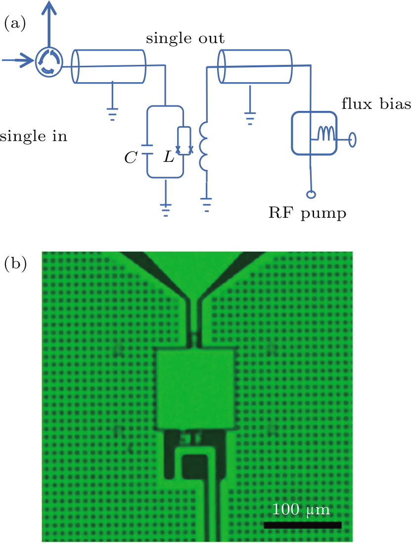 | Fig. 1. (color online) (a) A schematic diagram of our parameter amplifier. The circle represents the circulator in the measuring circuit. The circulator is used to separate the input signal and output signal. The cylinder represents 50 Ω signal input transmission line and on chip flux bias line. The square represents bias T to combine the RF pump and DC bias. (b) The optical micrograph of our Josephson parameter amplifier. The up triangle pad is the signal input pad, the center square is the parallel plate capacitor, and the down turning line is the on chip bias line. |
The amplification of Josephson junction based parametric amplifiers is based on the frequency mixing resulted from the nonlinear Josephson inductance. As the energy source, a sufficiently large pump mode is used to modulate the Josephson inductance of the system, in which the nonlinear Josephson junction plays a key role. During this process, the energy of the pump mode is transferred to the small incident signal mode, which results in the parametric amplification of the incident signal.
The bandwidth of the amplifier is limited by the resonator bandwidth that is inversely proportional to the coupled Q of the resonator to the environment. For a fixed environment impedance Z0 (which is typically 50 Ω for the transmission line) and resonant frequency ω0, the coupled Q ∼ Z0ω0L. In order to reduce Q, one may either increase L or decrease Z0. In this work, we followed the approach in Ref. [18] and fabricated a wide-band JPA by transforming the environmental impedance Z0 with a tapered impedance transformer. This approach leads to increased coupling, lowered Q, and simultaneously increased bandwidth and saturation power. The tapered impedance transformer is realized by shunting a CPW of fixed geometry with a series of parallel plate capacitor cross-overs. As pointed out in Ref. [18], the sections with a cross-over approximate a microstrip transmission line, with much lower local characteristic impedance. By varying the density of the cross-overs, the impedance can be varied smoothly.
The Josephson parametric amplifiers discussed here can be operated either in a three-wave mixing mode or a four-wave mixing mode.[18] In this work, we chose the three-wave mixing operation mode. In this mode, the signal is fed into the amplifier through the signal-in port while the pump is applied via the bias line along with the dc bias. The amplified output signal is reflected off the amplifier and sent to the next stage amplifier through the signal-out port. In order to separate the signal-in and signal-out ports, a circulator is used. When the frequency and the amplitude of the pump signal are in appropriate ranges, the nonlinear resonator runs in a parametric amplifier regime.[3–11]
The optical micrograph in Fig.
In Fig.
 | Fig. 2. (color online) (a) An optical micrograph of our wide band Josephson parameter amplifier. The up pad is the signal input pad, and the middle line is the signal transition line. With different density crossovers on the transmission line, the transmission line shows different colors from up to down, the crossover changes the impedance of the transmission line. (b) The Josephson parameter amplifier sampler mounted in a sample box. |
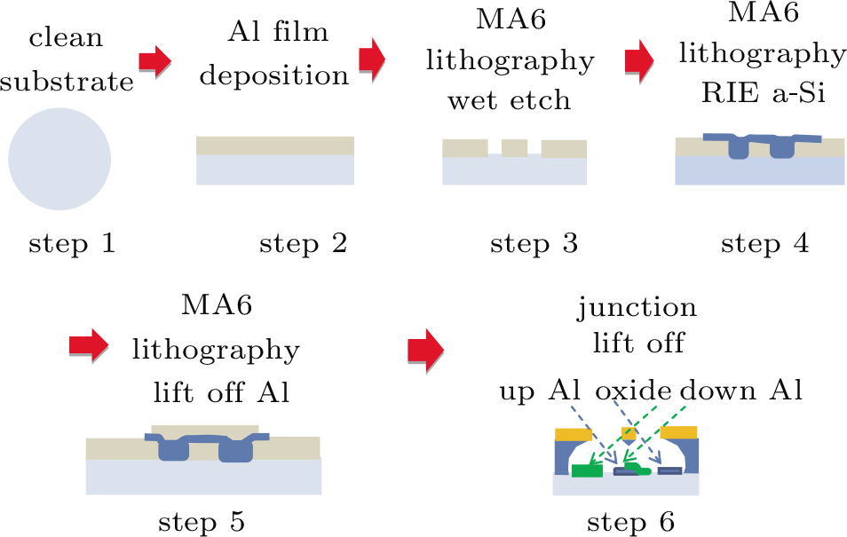
3. Sample fabrication process
We adopted a multilayer micro-fabrication process based on wet etching of Al for amplifier fabrication. In Fig.
 | Fig. 3. (color online) The schematic diagram of multilayer micro-fabrication process. |
The detailed steps are as follows. In the first step, we clean the high resistance silicon substrates (3000 Ω) sequentially in an ultrasonic bath using acetone, alcohol, and deionized water. In each clean, the clean time is about 10 min. In the second step, we deposit 100 nm thick aluminum using an ultra-high vacuum e-beam evaporation system (plasyss 520). In the third step, we use photo lithography (on a Kalsuss MA6 UV aligner) and wet etching to define the capacitor ground electrode, the signal input and output transmission line, the on-chip bias line, the meshed ground plane and position marks. The photo resist used in this step is S1813. For the wet etching process, we use type A solution (
Finally, we made the SQUID using a double-angle evaporation process.[22] The under-cut mask was made using two layers of resist (zip 520 and PMGI). A test SQUID was also made on the chip to check the junction room temperature resistance to see if the SQUID critical current is appropriated. The junction resistance is linked to the junction critical current by the Ambegaokar–Baratoff relation IC = πΔ/2eRn, where Δ is the superconducting energy gap of the electrode and Rn is the junction normal state resistance.
4. Sample characterization and properties analysis
For the characterization of JPAs, a fabricated Josephson parametric amplifier sample was mounted in an aluminum sample box and measured in a cryogen-free dilution refrigerator with a base temperature around 20 mK. The amplifier was operated in the phase preserving mode for the dispersive readout of Xmon qubits which were capacitively coupled to a transmission line through λ/4 coplanar waveguide resonators (CPW). The amplifier was connected to the qubit readout transmission line and the output of the amplifier was further amplified by a HEMT cryogenic amplifier operated at around 3 K, followed by a room temperature microwave amplifier.
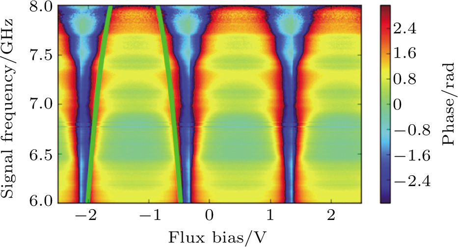
Before the measurement, we have measured the phase component of S21 versus the dc flux bias and signal frequency, where a periodic structure is observed due to the change of the SQUID critical current with the external magnetic flux. By varying the dc-flux, we can tune the resonant frequency of the nonlinear resonator into the regime for qubit readout. In Fig.
 | Fig. 4. (color online) The phase component of S21 versus dc flux bias and signal frequency of our wide-band JPA sample. |
Firstly, we present the results of a narrow-band JPA device. During the measurements, we recorded the S21 signal of the qubit readout transmission line. In Fig.
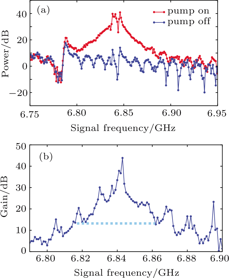 | Fig. 5. (color online) (a) The response of S21 of the quantum chip with Josephson parameter amplifier pump on and off. (b) Josephson parameter amplifier gain-bandwidth plot, the bandwidth with gain more than 14 dB is about 35 MHz. |
In order to further demonstrate the effectiveness of the amplifier for qubit readout, we present the data for different qubit states in Fig.
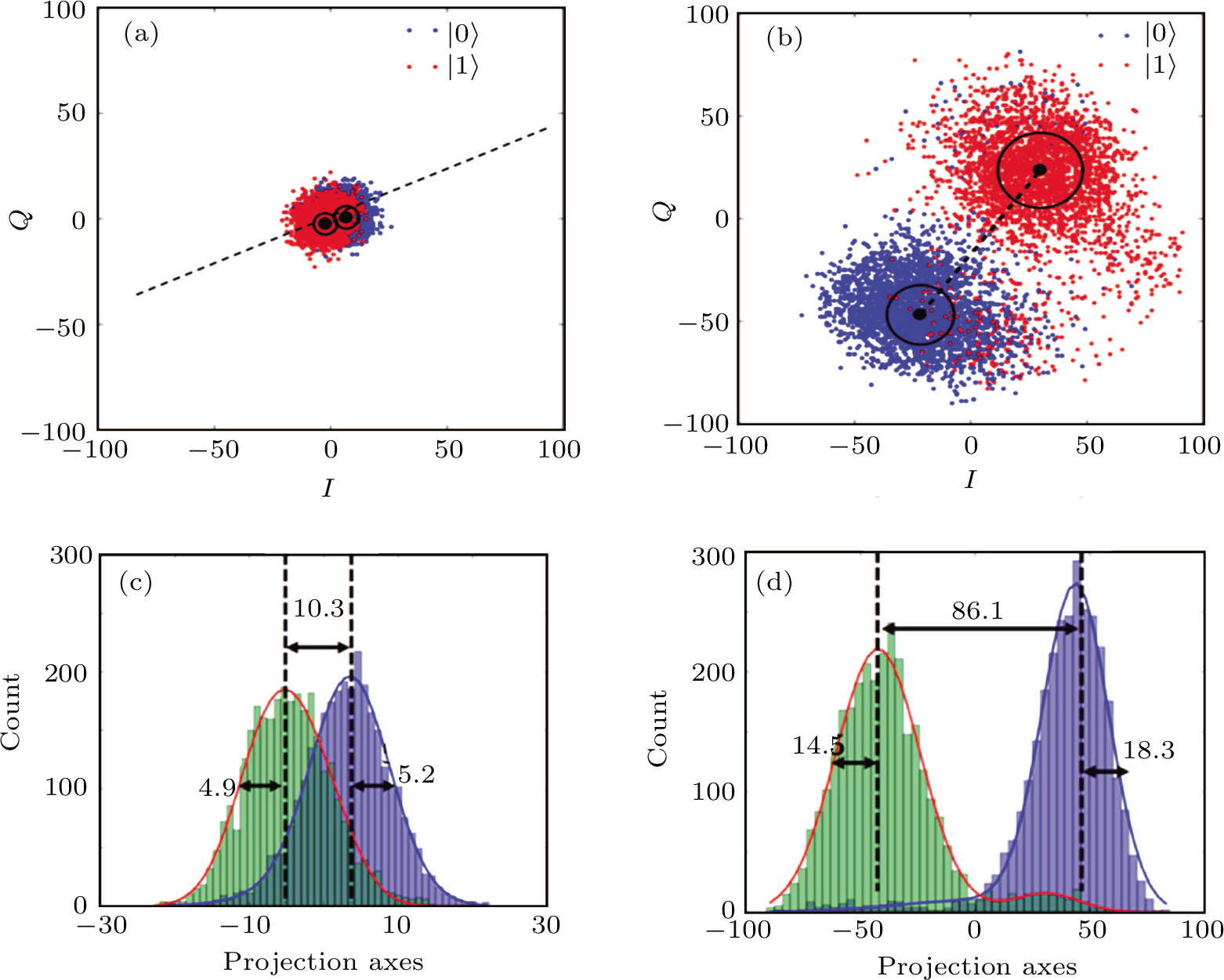 | Fig. 6. (color online) (a), (b) I–Q clouds for the qubit states measured with the JPA pump off and on. The color point represents the single short read out state |0〉 (blue) or |1〉 (red). The clouds represent the signal scatter by the noise. The bigger black points represent the average centers of the cloud points. The position of the bigger black point represents the position of the state without noise. The dash line connected the center represents the projection axes. The distance of the center represents the relative separation of readout states |0〉 and |1〉. (c), (d) The histograms of the readout points with JPA pump off and on, the outlines are Gaussian fits to the histograms and used to estimate the separation fidelity and measurement fidelity. We also estimate the JPA noise temperature by comparing the readout results with JPA off and on. |
The readout of the qubit state is based on the JC model that describes a system containing a two-level atom (qubit) coupled to a resonator. At the large detuning where the qubit and cavity frequency detuning Δ = ωq − ωr is much larger than the coupling rate g, the system Hamiltonian is 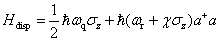
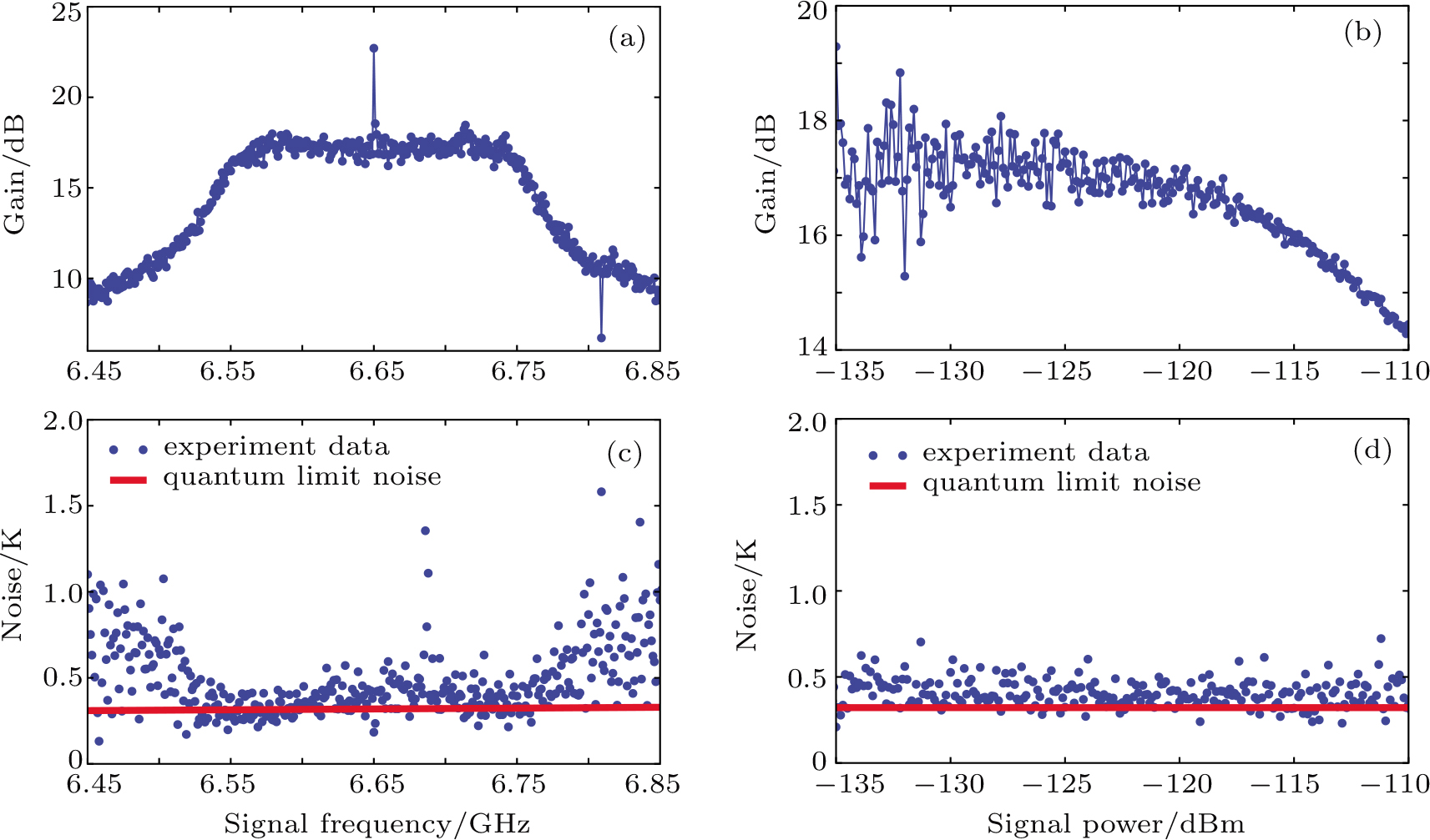
For the wide-band device, we performed similar measurements. In Figs.
 | Fig. 7. (color online) (a), (c) The frequency dependence of gain and noise; (b), (d) the signal power dependence of gain and noise. |
5. Conclusion
We have fabricated and characterized a narrow band and a wide band Josephson parametric amplifier. The devices consist of lumped elements and were made using a multilayer micro-fabrication process that is based on wet etch of aluminum films. The wet etching process has the advantage of not requiring the usage of toxic chlorine gas and expensive ICP systems. We believe that the process is therefore more suitable for small scale laboratories. For the narrow band JPA, the frequency band with gain larger than 14 dB is 35 MHz, while the wide band JPA shows over a 200 MHz range. The noise temperature of the JPAs is near the quantum limit. We used the JPA as pre-amplifier to readout superconducting qubit. The results show that the signal to noise ratio is improved significantly, and hence the measurement fidelity is improved.
Reference
| [1] | |
| [2] | |
| [3] | |
| [4] | |
| [5] | |
| [6] | |
| [7] | |
| [8] | |
| [9] | |
| [10] | |
| [11] | |
| [12] | |
| [13] | |
| [14] | |
| [15] | |
| [16] | |
| [17] | |
| [18] | |
| [19] | |
| [20] | |
| [21] | |
| [22] | |
| [23] | |
| [24] | |
| [25] | |
| [26] | |
| [27] |