Improved photovoltaic effects in Mn-doped BiFeO3 ferroelectric thin films through band gap engineering
Yan Tang-Liu1, 3, 4, Chen Bin3, 4, †, Liu Gang3, 4, Niu Rui-Peng2, Shang Jie3, 4, Gao Shuang3, 4, Xue Wu-Hong3, 4, Jin Jing1, ‡, Yang Jiu-Ru2, §, Li Run-Wei3, 4
School of Materials Science and Engineering, Shanghai University, Shanghai 200444, China
Electrical Engineering College, Heilongjiang University, Harbin 150080, China
Key Laboratory of Magnetic Materials and Devices, Ningbo Institute of Materials Technology and Engineering, Chinese Academy of Sciences, Ningbo 315201, China
Zhejiang Provincial Key Laboratory of Magnetic Materials and Application Technology, Ningbo Institute of Materials Technology and Engineering, Chinese Academy of Sciences, Ningbo 315201, China


† Corresponding author. E-mail: chenbin@nimte.ac.cn jjin@shu.edu.cn yangjr@hlju.edu.cn

Abstract

As a low-bandgap ferroelectric material, BiFeO3 has gained wide attention for the potential photovoltaic applications, since its photovoltaic effect in visible light range was reported in 2009. In the present work, Bi(Fe, Mn)O3 thin films are fabricated by pulsed laser deposition method, and the effects of Mn doping on the microstructure, optical, leakage, ferroelectric and photovoltaic characteristics of Bi(Fe, Mn)O3 thin films are systematically investigated. The x-ray diffraction data indicate that Bi(Fe, Mn)O3 thin films each have a rhombohedrally distorted perovskite structure. From the light absorption results, it follows that the band gap of Bi(Fe, Mn)O3 thin films can be tuned by doping different amounts of Mn content. More importantly, photovoltaic measurement demonstrates that the short-circuit photocurrent density and the open-circuit voltage can both be remarkably improved through doping an appropriate amount of Mn content, leading to the fascinating fact that the maximum power output of ITO/BiFe0.7Mn0.3O3/Nb-STO capacitor is about 175 times higher than that of ITO/BiFeO3/Nb-STO capacitor. The improvement of photovoltaic response in Bi(Fe, Mn)O3 thin film can be reasonably explained as being due to absorbing more visible light through bandgap engineering and maintaining the ferroelectric property at the same time.

1. Introduction

As a novel candidate of photovoltaic materials, ferroelectric materials have been extensively investigated, since Choi et al. reported the visible light range photovoltaic effect in bismuth ferrite (BiFeO3, shortened to BFO) in 2009.[1] Compared with the common photovoltaic effect in semiconductor p–n junction, the photovoltaic effect in ferroelectric has several unique characteristics: (i) the anomalous photovoltaic effect: as a result of the bulk photovoltaic effect, a large open circuit voltage can be obtained, which is much larger than the band gap;[2] (ii) the switchable photovoltaic response: the photocurrent and photovoltage direction can be switched upon external electric field, while it is impossible in conventional semiconductor p–n solar cells.[3] In contrast to the known semiconductor interfacial photovoltaic effect, the bulk photovoltaic effect in ferroelectric materials, promoted by the polarization-induced internal electric field, provides an opportunity to simplify the solar cell into a simple electrode/ferroelectric/electrode sandwich structure, without complicated junction structures.

Although the photovoltaic effect and several unique advantages in ferroelectrics have been known for more than half a century, these materials have not been considered for practical application to solar cells due to their small power conversion efficiencies, partly resulting from the relatively wide band gap of ferroelectric materials such as LiNbO3,[48] Pb(ZrTi)O3,[9,10] and BaTiO3.[11] The BFO with a relatively low bandgap of 2.67 eV has aroused great interest in the ferroelectric photovoltaic field.[1214] However photons with wavelength larger than 464 nm (accounting for more than 80% of the solar spectrum) cannot be absorbed by BFO materials either.[1,2,15,16] Recently, some novel ferroelectric materials with narrow band gap such as KBiFe (1.6 eV)[17] and [KNbO3] [BaNi0.5Nb ] (1.1 eV)[18] have been observed, which can effectively absorb visible light. However, the ferroelectric polarization of these materials is too low to separate the photo-exited carriers, which is detrimental for photovoltaic performance in ferroelectric materials.

Therefore, to achieve efficient ferroelectric-based photovoltaic devices, it is essential to balance both band gap and ferroelectric polarization, which promote the generation and separation of the photogenerated carriers. In 2014, Nechache et al.[19] experimentally reported that by tuning the Fe/Cr cationic ordering and domain size, the double perovskite Bi2FeCrO6 ferroelectric films can absorb the wide solar spectrum range from 1.4 eV to 3.2 eV and maintain the ferroelectric performance at room temperature, thereby providing a higher power conversion efficiency of 8.1% under AM 1.5 G irradiation (100 mW cm ). Actually, various doping elements have been considered for reducing the bandgap of BFO and absorbing more photon energy in solar energy, such as La, Nd, Sm, Pr, Dy, Cr, Mn. Among these eminent doping contributions, besides the Cr doping elements producing a higher photovoltaic response, it should be noted that Mn dopant element deserves to be further studied. Xu et al. have already proved that the bandgap of BFO can be straightforwardly tuned from 1.1 eV to 2.7 eV in Bi(Fe, Mn)O3 films, with the Mn element content varying from 100% to 0, which provides another potential candidate of ferroelectric material for photovoltaic materials.[20] However, few experimental results concerning the Mn dopant effect on the photovoltaic response in BFO film have been reported. Therefore, we fabricate various Mn element dopant BFO films by the pulsed laser deposition method and study the effects of Mn content on the microstructure, optical, ferroelectric and photovoltaic performance of BFO thin films systematically. We find that the photovoltaic response in ITO/Bi(Fe0.3Mn /Nb-STO film capacitor can be increased by almost 175 times than that in ITO/BiFeO3/Nb-STO film capacitor, due to absorbing more visible light and maintaining excellent ferroelectric performance in Bi(Fe, Mn)O3 films.

2. Experimental procedure

The BiFe Mn (x = 0, 0.1, 0.3 and 0.5) [shortened to BFMO] targets were synthesized via a solid state reaction route, where the starting materials were MnO2, Fe , and Bi . The Mn compositions in different ceramic targets were 0 mol%, 10 mol%, 30 mol%, and 50 mol% in total content of B-site element, respectively. The oxide mixture of BFMO composition was calcined at 700 °C in air for 2 h to form the desired BFMO phase, before it was sintered at 750 °C for 4 h to form the polycrystalline ceramic BFMO target. The 60-nm-thick BFMO ferroelectric films were grown on the (100)-orientation Nb-doped SrTiO3 substrates by the pulsed laser deposition at 560 °C and 9-Pa oxygen pressure, with a KrF excimer laser (248 nm, CoherentInc.) running at a repetition rate of 3 Hz and an energy density of 2.3 J/cm . We denote the samples with the Mn content values of 0 mol%, 10 mol%, 30 mol%, and 50 mol% as BM0, BM1, BM3, and BM5, respectively. In order to measure the electrical properties of the films, circular ITO top electrodes of 100 μm in diameter were deposited by the pulsed laser deposition method through shadow masks. The surface morphologies and ferroelectric property of the films were studied using an atomic force microscope (AFM, Veeco Dimension 3100V). The morphology measurements were made using an 8-nm diameter tip with k = 35 N/m, while a PtIr coated tip with k = 40 N/m for piezoresponse force microscopy (PFM) testing. The phases and textures of the films were determined by x-ray diffractometer (D8 Advance, Bruker) with Cu K radiation. Their leakage behaviors were characterized by using a Keithley meter 4200 parameter analyzer. The photovoltaic response performances were measured by a Keithley meter using a standard xenon lamp light source with an intensity of 85 W/m .

3. Results and discussion

Figure 1(a) shows the XRD patterns of the BFO thin films with different amounts of Mn doping content. Each of the BFMO films exhibits a strong (100) texture which is in accordance with the substrate orientation. Weak peaks of impurity phases (Bi and Bi2Fe are detected in BM0, BM1, and BM3, while the peaks of Bi in BM5 are much stronger. This result can be ascribed to the fact that Bi deficiencies are produced during migration of ablated species on the substrate before crystallization.[21,22] The enlarged view of Fig. 1(a) illustrates that the (100) diffraction peaks of BFMO shift towards higher diffraction angle gradually with increasing Mn content, which confirms the presence of lattice distortion in the previous reports.[2325] From the AFM topography images in Fig. 1(b), it is found that Mn substitution seems to affect the microstructure of the film. For the pure BFO film, the morphology of a quite smooth surface (with a surface roughness of 1.94 nm) is obtained. However, rough surface morphologies are found in Mn-doped BiFeO3 films, which display root-mean-square roughness values of about 4.44 nm, 8.76 nm, and 56.2 nm respectively. As a result, the surface roughness is remarkably increased with the increase of Mn content due to the formation of many nanoparticles.[21] This behavior seems to be mainly caused by the volatilization of Bi element, and the nanoparticles have been proved to be Bi phase.[26,27] Furthermore, we find that the Bi nano-pillar structures become larger with the increase of the Mn content, which is corresponding to the strong Bi peaks appearing in XRD pattern of BM5 sample.

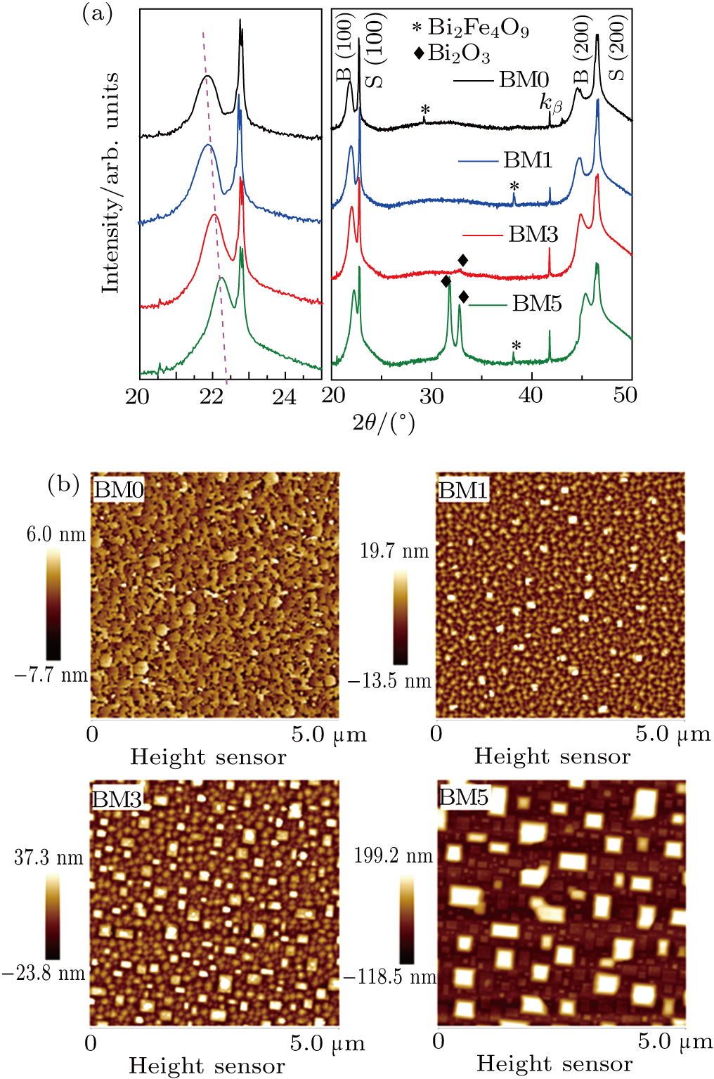
Fig. 1. (color online) (a) XRD
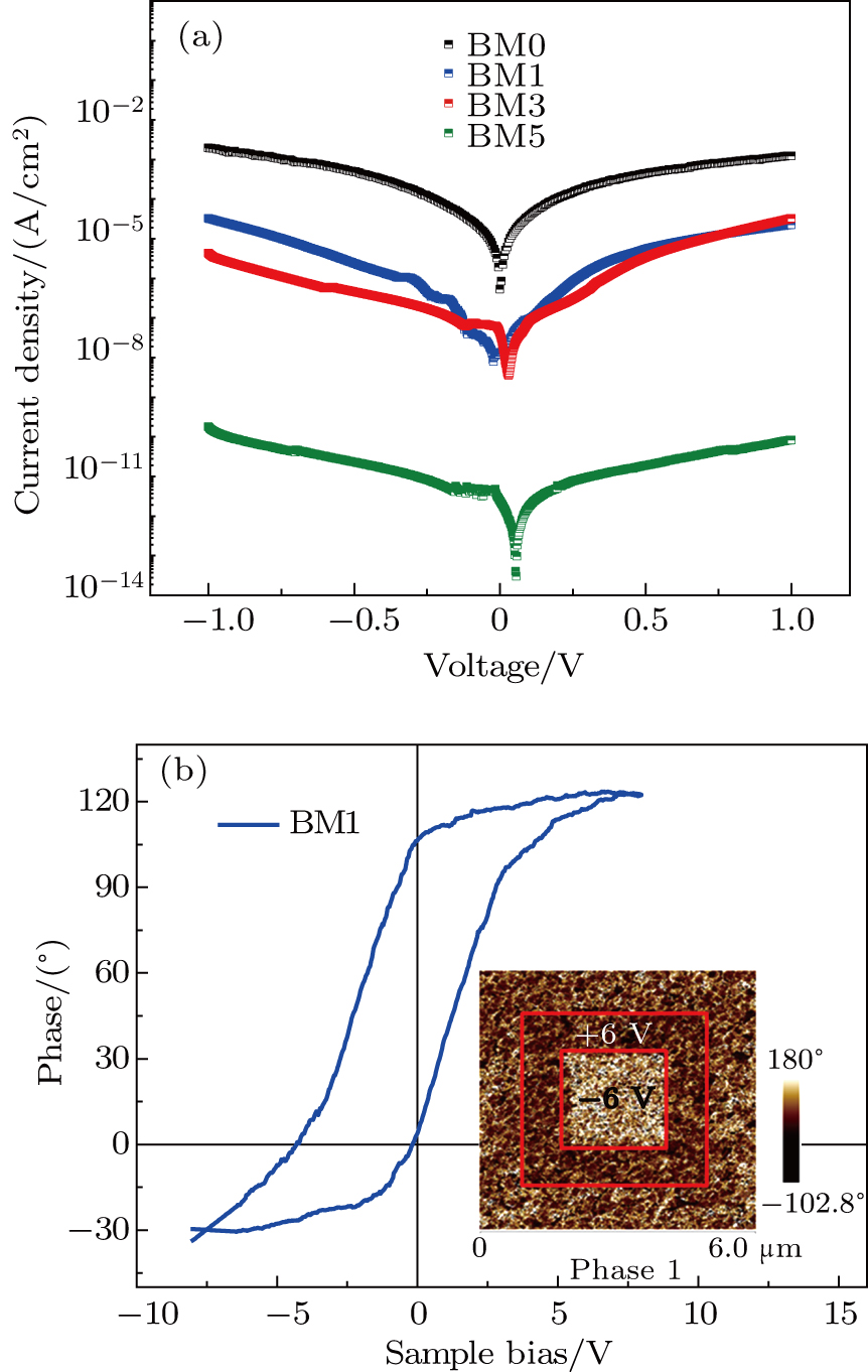
 –2 scan patterns of BiFeO3 (black), BiFe0.9Mn (blue), BiFe0.7Mn (red), and BiFe0.5Mn (green) thin films deposited on Nb-STO (100) substrates. The peaks are indexed as B for BFMO, S for Nb-STO. The left image is the enlarged view of XRD image. (b) AFM images of BiFe Mn O (x = 0, 0.1, 0.3, 0.5) thin films.

Figure 2(a) shows the plots of leakage current density versus input voltage of BFMO film capacitors doped with various amounts of Mn element content. The Mn-doped films each show a greatly reduced leakage current compared with pure film. The large leakage current density in BiFeO3 thin film is greatly associated with the presence of Fe and oxygen vacancies, while the leakage current density decreases remarkably due to the formation of deep traps.[28] The horizontal shift from zero in the leakage current curve may be due to the stored space charges at the electrodes/BiFeO3 interface, which was also investigated in other papers.[29,30] Furthermore, we demonstrate that the device interface contact is of Schottky barrier mode through fitting the IV curve at different temperatures. As mentioned before, the separation of the photo-excited carriers in ferroelectric films results from the ferroelectric induced depolarization field. In order to check the ferroelectric performance in a BFMO film, the piezoelectric force microscope method is used. Figure 2(b) exhibits a clear loop of local response of the phase to the bias field and the inset shows the switchable out-plane domain piezoresponse force microscopy image under plus or minus 6-V bias in BM1, all of these are the evidence of ferroelectric polarization switching. It should be mentioned that this switchable ferroelectric performance can be observed in all BFMO films, which is critical for the photovoltaic applications in ferroelectric films.

Fig. 2. (color online) (a) Plots of current density versus input voltage in Bi(Fe,Mn)O3 films doped with various amounts of Mn element content. (b) PFM piezoelectric response phase loop for BM1 sample. The insert is ferroelectric domains image of BM1 sample after applying -V poling bias.

Besides the ferroelectric properties of BFMO films, the property of light absorption is critical to improving the photovoltaic response. Figure 3 shows the room-temperature absorption spectra of the BFMO films doped with various amounts of Mn element content. Absorption coefficient is calculated from , where d is the film thickness, is the measured transmittance, and E is the energy, respectively. It is preceded by a small shoulder centered at eV, which yields an absorption onset near 2.00 eV in BM0 sample. First, the small shoulder at 2.25 eV is broadened obviously and begins to be red-shifted with the increase of Mn content. For each of BM0 and BM1 samples, the onset of optical absorption is near 2.00 eV, however, for the BM3 it is about 1.9 eV. Then, the shoulder at 3.2 eV becomes intense and obvious with Mn content increasing. The direct band gap is extracted by linearly extrapolating the plot of ( versus E to zero (as shown in the insert). We find that the direct band gap values are at 2.86 eV, 2.82 eV, 2.71 eV in BM0, BM1, BM3 samples respectively, the bandgap variation tendency is consistent with that of the results by Xu et al.[20] However, the BM5 sample exhibits the less light absorption performance than the BM3 sample. The reason for the small absorption in the BM5 is not clear at this moment. It is clear that BiFeO3 films doped with Mn element can improve the performance of the spectrum absorption in visible light, which is significantly beneficial to the light-to-electricity conversion process due to the fact that more photo-induced carriers are generated. This may provide an effective candidate of photovoltaic material for potential solar cell applications.

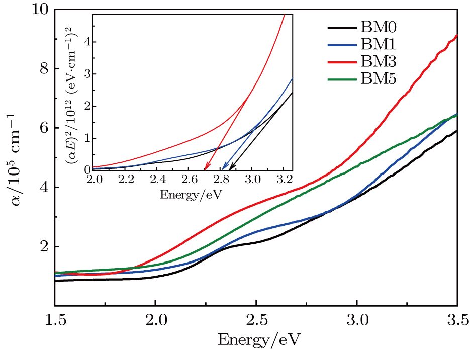
Fig. 3. (color online) Variations of absorption coefficient with energy of Bi(Fe, Mn)O3 films on the quartz substrates. The insert image shows the direct band gap analyses of these thin film samples.

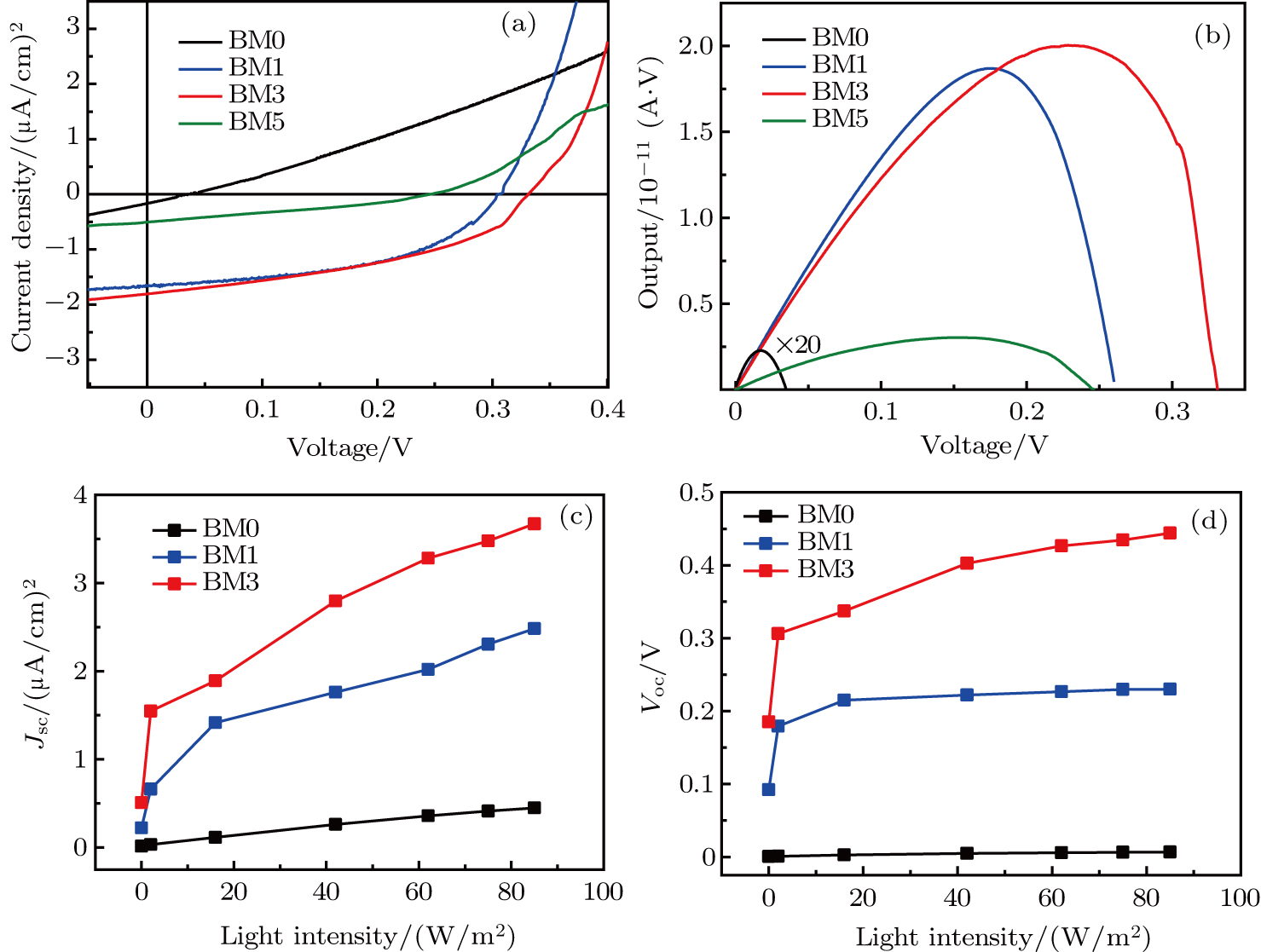
The photovoltaic responses in various ITO/Bi(Fe, Mn)O3/Nb-STO film capacitors are measured [Fig. 4(a)], indicating an improved photovoltaic response in Mn-doped BFO film. The photocurrent density ( of 0.17 μA/cm and photovoltage ( of 0.04 V are exhibited under 85-W/m illumination conditions in BM0 sample and subsequent larger and values are obtained in Mn-doped samples. Meanwhile, the values of and are improved to 1.66 μA/cm and 0.31 V in BM1, 1.81 μA/cm and 0.33 V in BM3, respectively. However, the and are 0.5 μA/cm and 0.25 V in BM5, which is probably due to the formation of higher content of impurity phase (Bi as shown in the XRD pattern and AFM image (see Fig. 1). Figure 4(b) shows the corresponding terminal voltage dependence of output for various ITO/Bi(Fe, Mn)O3 Nb-STO capacitors. By comparison with BM0 capacitor, the output power of Mn-doped BiFeO3 film is much higher. Specifically, the output power value of the ITO/Bi(Fe0.7Mn Nb-STO capacitor is almost 175 times larger than that of the ITO/BiFeO3/Nb-STO capacitor. The variations of and with illumination intensity are also shown in Figs. 4(c) and 4(d). Apparently, the values of and are both proportional to incident light intensity as shown in Figs. 4(c) and 4(d). The is observed to increase almost linearly with the illumination intensity rising (Fig. 4(c)), while becomes saturated gradually with illumination intensity increasing (Fig. 4(d)). These variation trends are similar to those of the semiconductor solar devices.[31]

Fig. 4. (color online) (a) Plots of current density versus the input voltage of Bi(Fe, Mn)O3 films with visible light at 85 W/m . (b) Corresponding terminal voltage dependence of output (voltage current) for ITO/Bi(Fe, Mn)O3/Nb-STO capacitors. (c) Plots of short-circuit current density, versus light intensity. (d) Plots of open-circuit voltage, versus light intensity.
4. Conclusions

In this work, the effects of doping Mn on the microstructure, optical, leakage, ferroelectric and photovoltaic characteristics in BFO films are investigated systematically. Optical measurements demonstrate that the bandgap and the light absorption performance can be effectively tuned by doping various amounts of Mn content. From the photovoltaic results, it is clear that the photovoltaic output in ITO/Bi(Fe /Nb-STO capacitor is almost 175 times larger than that in ITO/BiFeO3/Nb-STO capacitor. Our experimental results demonstrate that Mn element doping would be an effective method to improve the photovoltaic response of BiFeO3 film.

Reference
[1] Choi T Lee S Choi Y J Kiryukin V Cheong S W 2009 Science 324 63
[2] Yang S Y Seidel J Byrnes S J Shafer P Yang C H Rossell M D Yu P Chu Y H Scott J F Ager J W Martin L W Ramesh R 2010 Nat. Nanotechnol. 5 143
[3] Ji W Yao K Liang Y C. 2010 Adv. Mater. 22 1763
[4] Glass A M Von der Linde D Negran T J 1974 Appl. Phys. Lett. 25 233
[5] Arizmendi L 2004 Phys. Status Solidi 201 253
[6] Glass A Von der Linde D Auston D Negran T 1975 J. Electron. Mater. 4 915
[7] Carnicero J Caballero O Carrascosa M Cabrera J 2004 Appl. Phys. 79 351
[8] Kang B Rhee B K Joo G T Lee S Lim K S 2006 Opt. Commun. 266 203
[9] Ichiki M Morikawa Y Nakada T 2002 Jpn. J. Appl. Phys. 41 6993
[10] Ichiki M Maeda R Morikawa Y Mabune Y Nakada T Nonaka K 2004 Appl. Phys. Lett. 84 395
[11] Spanier J E Fridkin V M Rappe A M Akbashev A R Polemi A Qi Y B Gu Z Q Young S M Hawley C J Imbrenda D Xiao G Bennett-Jackson A L Johnson C L 2016 Nat. Photon. 10 611
[12] Ji W Yao K Liang Y C 2010 Adv. Mater. 22 1763
[13] Luo B C Chen C L Fan F Jin K X 2012 Chin. Phys. Lett. 29 018104
[14] Zhou Y E Tan X Y Yu B F Liu L Yuan S L Jiao W H 2014 Chin. Phys. Lett. 31 037304
[15] Ji W Yao K Liang Y C 2011 Phys. Rev. 84 094115
[16] Nechache R Harnagea C Licoccia S Traversa E Ruediger A Pignolet A Rosei F 2011 Appl. Phys. Lett. 98 202902
[17] Zhang G H Wu H Li G B Huang Q Z Yang C Y Huang F Q Liao F H Lin J H 2013 Sci. Rep. 3 1265
[18] Grinberg I West D V Torres M Gou G Y Stein D M. Wu L Y Chen G N Gallo E M Akbashev A R Davies P K Spanier J E Rappe A M 2013 Nature 503 509
[19] Nechache R Harnagea C Li S Cardenas L Huang W Chakrabartty J Rosei F 2014 Nat. Photon. 9 61
[20] Xu X S Ihlefeld J F Lee J H Ezekoye O K Vlahos E Ramesh R Gopalan V Pan X Q Schlom D G Musfeldt J L 2010 Appl. Phys. Lett. 96 192901
[21] Béa H Bibes M Barthélémy A Bouzehouane K Khodan A Contour J P Fusil S Wyczisk F Forget A Lebeugle D Colson D Viret M 2005 Appl. Phys. Lett. 88 062502
[22] Béa H Bibes M Fusil S Bouzehouane K Jacquet E Rode K Bencok P Barthélémy A 2006 Phys. Rev. 74 020101
[23] Wen Z Hu G D Fan S H Yang C H Wu W B Zhou Y Chen X M Cui S G 2009 Thin Solid Films 517 4497
[24] Ding N F Deng H M Yang P X Chu J H 2012 Mater. Lett. 82 71
[25] Singh S K Ishiwara H Sato K Maruyama K 2007 J. Appl. Phys. 102 094109
[26] Béa M. Bibes A Barthélémy H Bouzehouane K Jacquet E Khodan A Contour S Fusil F Wyczisk A Forget J P Lebeugle D Colson D Viret M 2005 Appl. Phys. Lett. 87 072508
[27] Alexe M Scott J F Curran C Zakharov N D Hesse D Pignolet A 1998 Appl. Phys. Lett. 73 1592
[28] Kawae T Terauchi Y Tsuda H Kumeda M Morimoto A 2009 Appl. Phys. Lett. 94 112904
[29] Wei L J Sun B Zhao W X Li H W Chen P 2017 Appl. Surf. Sci. 393 325
[30] Wu J G Wang J Xiao D Q Zhu J G 2011 Mater. Res. Bull. 46 2183
[31] Liu E K Zhu B S Luo J S 2011 The Physics of Semiconductors 7 Beijing Publishing House of Electronics Industry 296