

Ballistic transport and quantum interference in InSb nanowire devices
Cite this Article
Li Sen, Huang Guang-Yao, Guo Jing-Kun, Kang Ning, Caroff Philippe, Xu Hong-Qi. Ballistic transport and quantum interference in InSb nanowire devices. Chinese Physics B, 2017, 26(2): 027305 
Permissions
Ballistic transport and quantum interference in InSb nanowire devices
† Corresponding author. E-mail:
Project supported by the National Key Basic Research and Development Project of the Ministry of Science and Technology of China (Grant No. 2016YFA0300601) and the National Natural Science Foundation of China (Grant Nos. 91221202, 91421303, 11374019, and 61321001).
Abstract
An experimental realization of a ballistic superconductor proximitized semiconductor nanowire device is a necessary step towards engineering topological quantum electronics. Here, we report on ballistic transport in InSb nanowires grown by molecular-beam epitaxy contacted by superconductor electrodes. At an elevated temperature, clear conductance plateaus are observed at zero magnetic field and in agreement with calculations based on the Landauer formula. At lower temperature, we have observed characteristic Fabry–Pérot patterns which confirm the ballistic nature of charge transport. Furthermore, the magnetoconductance measurements in the ballistic regime reveal a periodic variation related to the Fabry–Pérot oscillations. The result can be reasonably explained by taking into account the impact of magnetic field on the phase of ballistic electron’s wave function, which is further verified by our simulation. Our results pave the way for better understanding of the quantum interference effects on the transport properties of InSb nanowires in the ballistic regime as well as developing of novel device for topological quantum computations.
1. Introduction
Semiconductor nanowires are appealing candidates for constructing novel devices in nanoelectronics.[1] Among them, InSb nanowires have been investigated for applications in high-speed electronics,[2] spintronics,[3] and quantum computing,[4,5] due to their remarkable properties such as a high electron mobility, a strong spin–orbit coupling,[6] and a large Landé g-factor,[7–9] Recently, it has been theoretically proposed[10,11] and experimentally realized[12,13] that hybrid devices based on these nanowires can be made as hosts for Majorana bound states (MBS) in solid state. Beside the essential ingredients such as proximity induced superconductivity and strong spin-orbit coupling, the ballistic transport inside the nanowire with the tunability of one-dimensional (1D) modes is also a key requisite and is seldom explored. For ballistic transport in 1D systems, quantized conductance plateaus emerge as a result of the 1D subband spectrum and have been routinely observed in constrictions formed in two-dimensional electron gas (2DEG).[14,15] Besides, the coherent electron waves traveling inside a ballistic channel can have interference effect, leading to a Fabry–Pérot pattern in the conductance spectroscopy. Such patterns have been well observed and used as siganatures of ballistic transport in carbon nanotubes[16,17] and in III– V nanowires.[18–20] Very recently, quantized conductance in InSb nanowires at zero magnetic field has been demonstrated with normal metal contacts.[21] However, an extensive and direct demonstration on the ballistic nature of superconductor contacted nanowire device remains challenging and largely unexplored.
Here, we report on the ballistic transport behavior in InSb nanowires with superconductor contacts. In this work, we focus on measurements of the devices in the normal state either at a high temperature (> Tc) or with a small magnetic field (> Bc) applied. We observe well defined conductance plateaus in the InSb nanowire device at an elevated temperature, which is a direct signature of ballistic transport in the nanowire and can be well described by the Landauer approach. Through analysis of consistent fitting, a mean free path le ≈ 90 nm is extracted. At lower temperature, conductance oscillations as a result of the Fabry–Pérot interference are observed and characterized with bias spectroscopy. We further measure the low temperature magnetoconductance patterns in Fabry–Pérot regime. The evolution of magnetoconductance as a function of gate voltage can be attributed to the quantum interference effects in such a ballistic system. Previous magnetotransport measurements have been utilized in nanowires to study phase coherent processes and extract various mesoscopic length scales.[22–24] However, most of them have been carried out in the diffusive regime with few efforts on the (quasi) ballistic regime.[25,26] Our result can be well understood by considering a phase shift induced by the magnetic field, which reveals the quantum interference nature of the transport process.
2. Experiment
InSb nanowires investigated in this study are grown by gold catalyzed gas-source molecular beam epitaxy on InP(111)B substrate following the growth of a stem segment of InAs.[9] The InSb nanowires have diameters of 50 nm–80 nm and lengths up to 3 µm, exhibiting a pure zinc blende crystal structure, free from twin defects and tapering.[27,28] After growth, the InSb nanowires are mechanically transferred onto an n++-doped Si substrate with an 110-nm thick thermally oxided top layer used as a global back gate. Ti/Al (5 nm/90 nm) contacts are patterned on the located individual InSb nanowires by standard electron beam lithography, followed by e-beam evaporation and lift-off processes. Before contact deposition, the nanowires are treated with a brief sulfur passivation process to remove the surface oxide and meliorate the contact interface. The superconducting contacts have been characterized in our previous work to have a critical temperature Tc ~ 1 K and a critical field Bc ~ 25 mT.[19] The devices studied in this work have contact separations of 60 nm–100 nm and diameters of 60 ± 5 nm. A typical scanning electron microscope image of devices investigated in this work is shown in Fig.
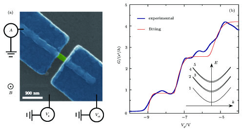 | Fig. 1. (color online) (a) False-color SEM image of a typical InSb nanowire device. The InSb nanowire (green) of typical diameter 60 ± 5 nm is contacted by two Ti/Al (5 nm/90 nm) superconducting electrodes. The contact spacings are in a range of 60 nm–100 nm. (b) Differential conductance G as a function of back gate voltage Vg measured at T = 10 K and B = 0 T using an ac bias Vac = 100 µeV (blue curve). Red curve is a fit to the experimental data based on the Landauer formula of conductance. Inset: schematic of the 1D subbands of an InSb nanowire. The second and third as well as the fourth and fifth subband are nearly degenerate owing to an additional symmetry of the nanowire discussed in the main text. |
3. Results and discussion
4(b) . It is clear that the main features of the experimental result can be well reproduced by this model, which therefore strongly supports our interpretation.
We first show the results of a device with a nanowire diameter d ~ 60 nm and a contact spacing L ~ 70 nm. The conductance G as a function of the back gate voltage Vg measured by ac method at a temperature of 10 K and zero magnetic field is plotted in Fig.
where f (E) is the Fermi–Dirac distribution. The summation comprises all the degenerate subbands contributing to the transport and Ti(E) is their transmission coefficient. The function between EF and Vg is established through the relation that the integrated density of states equal to the number of gate voltage-induced carriers per unit length
where Cg is the gating efficiency of the back gate and VT is the threshold voltage. We use this model to fit our data with Cg, Ti, and the subband spacing ∆Ei,i+1 as fitting parameters and the corresponding result is shown as the red curve in Fig.
Next we turn to another device with a similar nanowire diameter but a longer channel length L ~ 90 nm. Here we measured the device at a lower temperature of T ~ 10 mK, enabling us to investigate more of the quantum interference effects in the InSb nanowire. Since the Ti/Al contacts become superconducting at such low temperature, we apply a small magnetic field (50 mT) to suppress superconductivity in the Al contacts. The normal state transfer curve G(Vg) is presented in Fig.
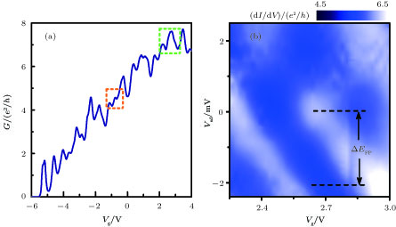 | Fig. 2. (color online) (a) Conductance G of a second device as a function of back gate voltage Vg measured at T = 10 mK with an ac bias Vac = 100 µeV. A small magnetic field B = 30 mT is applied to suppress superconductivity in the Al contacts. Green and orange squares mark the regions to be discussed hereinbelow. (b) Differential conductance dI/dV as a function of bias voltage Vsd and gate voltage Vg, corresponding to the same range denoted by the green square in panel (a). The nonlinear transport spectroscopy shows a characteristic Fabry–Pérot interference pattern, providing direct experimental evidence for ballistic charge transport through InSb nanowires. |
To better characterize the observed quasi-periodic conductance oscillations, we perform transport spectroscopy by measuring the differential conductance dI/dV as a function of Vsd and Vg in a typical region of oscillatory conductance (green dashed square in Fig. 
where ∆EFP is the energy spacing of the virtual resonant states from the constructive Fabry–Pérot interference. From Fig. 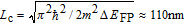
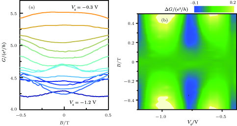
Having demonstrated the ballistic transport regime in our device, we move on to study quantum interference effects on the conductance in the presence of a magnetic field. We focus on a region displaying the Fabry–Pérot oscillations (orange dashed square in Fig.
 | Fig. 3. (color online) (a) Magnetoconductance (MC) traces measured at a temperature of 10 mK from Vg = −1.2 V to Vg = −0.3 V, corresponding to the same region denoted by the orange square in Fig. |
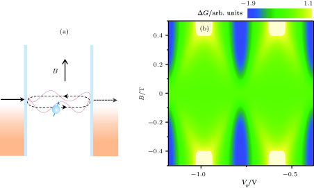
Based on this scenario, the evolution of gate-tuned magnetoconductance can be understood quantitatively on the basis of a simple model shown schematically in Fig.
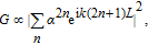
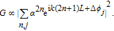
 | Fig. 4. (color online) (a) Schematic diagram of the transport model of electrons in a ballistic metal–nanowire–metal device under a perpendicular magnetic field. As a result of ballistic regime, electrons get only reflected at the two interfaces. The red curve refers to the electron wave of the interference process. (b) Simulated subtracted magnetoconductance ∆G as a function of the gate voltage and the magnetic field. The results show a good qualitative agreement with the experimental measurements shown in Fig. |
4. Conclusion
In conclusion, we have demonstrated comprehensive evidences for the ballistic transport in superconductor contacted InSb nanowires devices. We observe clear plateaus of conductance in a nanowire at a temperature of 10 K and zero magnetic field with the ability to accurately control the population of the 1D subbands. At a lower temperature, we have observed characteristic Fabry–Pérot resonances which confirm the ballistic nature of charge transport in the InSb nanowire. We further demonstrate the quantum interferences effects on the conductance of nanowire in the presence of a magnetic field. The magnetoconductance data in the Fabry–Pérot regime can be well explained by considering the phase shift induced by the magnetic field in a ballistic nanowire, which is further verified by our simulation. Given the strong spin-orbit interaction in InSb nanowires, more exotic features of transport, such as the helical modes,[32] deserve attention in such systems in future studies. Our results pave the way towards tailoring the desired 1D topological modes and understanding of coherent transport in superconductor contacted InSb nanowires.
Reference
| [1] | |
| [2] | |
| [3] | |
| [4] | |
| [5] | |
| [6] | |
| [7] | |
| [8] | |
| [9] | |
| [10] | |
| [11] | |
| [12] | |
| [13] | |
| [14] | |
| [15] | |
| [16] | |
| [17] | |
| [18] | |
| [19] | |
| [20] | |
| [21] | |
| [22] | |
| [23] | |
| [24] | |
| [25] | |
| [26] | |
| [27] | |
| [28] | |
| [29] | |
| [30] | |
| [31] | |
| [32] |