Ballistic transport and quantum interference in InSb nanowire devices
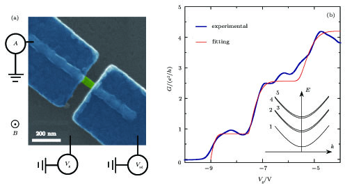
(color online) (a) False-color SEM image of a typical InSb nanowire device. The InSb nanowire (green) of typical diameter 60 ± 5 nm is contacted by two Ti/Al (5 nm/90 nm) superconducting electrodes. The contact spacings are in a range of 60 nm–100 nm. (b) Differential conductance G as a function of back gate voltage Vg measured at T = 10 K and B = 0 T using an ac bias Vac = 100 µeV (blue curve). Red curve is a fit to the experimental data based on the Landauer formula of conductance. Inset: schematic of the 1D subbands of an InSb nanowire. The second and third as well as the fourth and fifth subband are nearly degenerate owing to an additional symmetry of the nanowire discussed in the main text.