1. IntroductionThe rapid downscaling of metal–oxide–semiconductor field-effect transistors (MOSFETs) has posed increasing challenges such as short channel effect and degenerated carrier mobility. In particular, the ultrasharp pn junction with extremely high doping gradients becomes difficult to manufacture as the gate length is reduced down to 10 nm or even less. The junctionless nanowire transistor (JNT) has been recently proposed as a promising alternative to a new generation of transistors.[1,2] The doping concentration of JNT is uniform through the source, channel and drain. The current flows through the bulk of the channel as opposed to just along the surface in comparison with junction-based inversion-mode MOSFET. Consequently, JNT exhibits more excellent electrical performances. The key to fabricating JNT is the formation of an ultra-narrow channel to ensure the full depletion of carriers under zero gate voltage.
For decades, photolithography has been the predominant method of fabricating MOSFETs. Photolithography uses light to transfer a patterned feature from a photomask to photoresist on semiconductor wafer. Since the cost for lithographic equipment and photomask sets keeps rising with each technology generation, alternative cheaper patterning techniques are urgently required. The nanofabrication utilizing laser as an energy source has a multitude of advantages including maskless, three dimensions, high resolution and rapid prototyping,[3,4] providing an attractive method for nanoscale patterning applications. Early experimental results showed that the nanostructures fabricated by laser ablation always have thermal damages. However, femtosecond laser lithography can transform the photoresist by absorbing one or multiple phonons, which will dramatically reduce the thermal damages. In this approach, the focused femtosecond laser is directly used to write the desired image into the photoresist without lithographic mask. Thus, it offers great flexibility due to its maskless and discretionary nature. Previous theoretical and experimental results have proved that the multiphoton nanofabrication has the potential to exceed the diffraction limit.[5] Besides, the interaction between the femtosecond laser and the material occurs only in the vicinity of focal spot, leaving material surface intact. This manufacturing technique has been successfully utilized to fabricate nanoscale dot arrays and lines in silicon wafers.[6,7]
In this paper, we demonstrate the experimental results of JNT fabricated by femtosecond laser two-photon lithography. Two laser beams are focused by an optical lens system to be a writing spot on the wafer surface, which provides the optical energy for transforming the photoresist. Two dry etching processes are implemented to transfer the desired image from the negative SCR500 resin onto the top silicon layer. The fabricated JNT exhibits good gate control ability, large electron mobility, and good low-temperature instability.
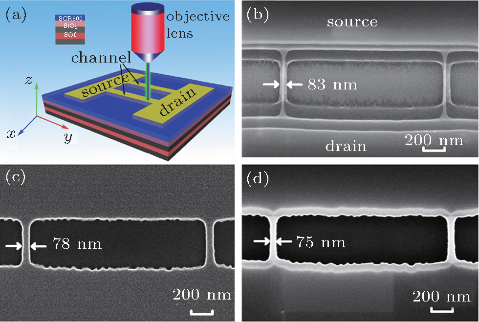
2. Device fabricationThe starting material was a (100)-oriented SOI wafer with a 55-nm-thick top silicon and a 145-nm-thick buried oxide. Two laser beams with the peak wavelengths of 800 nm and 400 nm were utilized to fabricate the device. The pulse width and repetition rate were 100 fs and 82 MHz, respectively. The top silicon layer was uniform heavily doped by phosphorus ion implantation with a dose of 5 × 1013 cm−2, leading to a doping concentration of 1 × 1019 cm−3. It was followed by depositing a 50-nm-thick SiO2 layer on the top of SOI substrate. The SiO2 layer was chosen to minimize the standing wave effect of the femtosecond laser.[8] Afterwards, femtosecond laser lithography with optimized laser powers of 3.38 mW for 800 nm laser and 2.02 μW for 400 nm laser was utilized to linearly pattern twin nanowires connecting two pads, as illustrated in Fig. 1(a). The speed of transportation of the sample in this process was 80 μm/s. The laser beams focused by an objective lens with a numerical aperture of 1.45 were scanned onto the substrate covering negative SCR500 resin by adjusting the position of translational stage. The photoresist was exposed via two-photon absorption in the area where the laser beams scanned across the photoresist. Figure 1(b) shows the scanning electron microscopy (SEM) image of the patterned photoresist mask. The desired image was transferred from the negative photoresist onto top silicon layer by two-step inductively coupled plasma (ICP) etching process. First, the deposited SiO2 layer was etched with the exposed photoresist as hard mask. Afterwards, the top silicon layer was etched with SiO2 as hard mask. The patterned SiO2 mask is shown in Fig. 1(c). After the etching step, SiO2 layer was removed by 5% HF. The SEM image presented in Fig. 1(d) shows that the width of nanowire with smooth surface is about 75 nm on average and the length of nanowire is 500 nm. The transfer line width after etching top silicon layer reduced 8 nm in comparison with the exposed line width on the photoresist. Then the sample was oxidized in dry oxygen at 900 °C for 1 h, resulting in the formation of silicon fin with a height of 28 nm (H) and width of 55 nm (W). The thickness of SiO2 gate dielectric formed by thermal oxidation was about 22 nm. The length of patterned heavily arsenic doped poly-silicon gate was 320 nm (L).
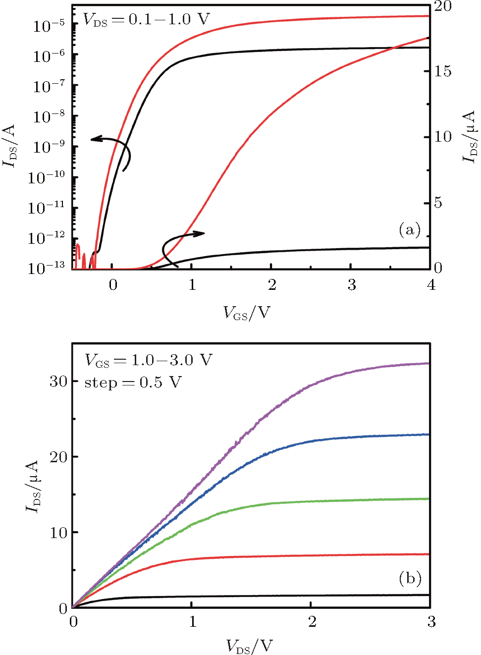
3. Results and discussion3.1. Electrical properties at room temperatureThe electrical characteristics of JNT are characterized by Agilent B1500 semiconductor parameter analyzer. Low temperature characterizations are carried out by Lakershore-340 temperature controller under high vacuum. At room temperature, the silicon JNT exhibits good transfer and output characteristics. The curves of drain current IDS versus gate voltage VGS in Fig. 2(a) show that the fabricated JNT operates as a normally-off device with a low gate leakage current of several pA. The SS and the threshold voltage (Vth) are 140 mV/dec and 0.68 V, respectively. The on/off current ratio is large than 1 × 10⁷.
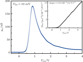
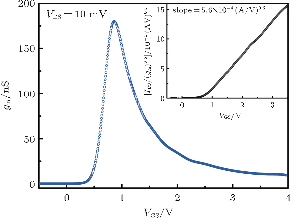
The plot of the extracted transconductance (gm = ∂IDS/∂VGS) versus VGS from transfer characteristics at VDS = 10 mV is shown in Fig. 3. The low-field electron mobility μ0 is extracted in linear part by using  method, which is independent of the series resistance and mobility attenuation factor, and expressed by[9]

Here
Cox, is the gate capacitance per unit area and estimated to be 1.56 × 10
7 F/cm
2 for 22-nm-thick gate oxide layer,
L is the gate length, and
Weff = 2(
W + 2
H) is the effective width for twin silicon nanowires. The inset of Fig.
3 shows the corresponding plot of the

as a function of
VGS. The extracted low-field mobility at
VDS = 10 mV is 290 cm
2·V
−1·s
−1. This suggests that the femtosecond laser lithography can impede damages normally introduced by high thermal density in laser ablation process, resulting in enhanced electron mobility in JNT.
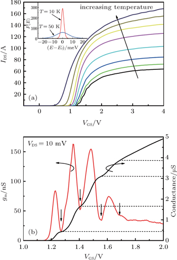
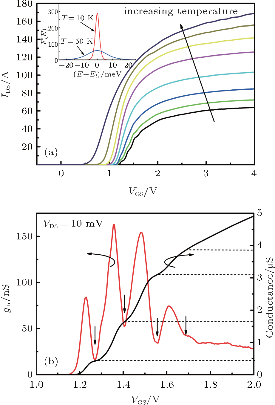
3.2. Temperature-dependent transfer characteristicsNext, we focus on the temperature-dependent transport of JNT. When the temperature is reduced, the interesting electrical results are observed. Figure 4(a) shows the measured transfer characteristics of JNT with VDS = 10 mV at different temperatures. The IDS decreases with temperature decreasing. Significantly, the transfer characteristic exhibits stepwise features below temperature ∼50 K, as a result of the Fermi energy Ef being tuned through the density of states (DOS) peaks of 1D subbands.[10] However, the step-like feature is found to be smeared out with the thermal smearing of 1D energy levels above 50 K. This is because the thermal broadening (kBT) at 50 K are too large to distinguish the energy separation between quantized subbands, where kB is the Boltmann constant.[11] Figure 4(b) shows the transfer curve and the corresponding transconductance gm as a function of VGS at the low temperature of 10 K. The black arrows mark the fixed gate voltage positions for the gm valleys. The positions correspond to the gate voltages of 1.27 V, 1.41 V, 1.56 V, and 1.74 V. The dotted lines mark the corresponding conductance heights. The height ratio of four current steps is 0.70:2.00:2.34:1.00. The heights of the first and fourth current step are approximately half the second step and half the third step, respectively, which infers that the second and third subband are two-fold degenerate with respect to the other two subbands. The interesting observation can be ascribed to the splitting of equivalent valley in silicon conduction band. The six valleys of silicon are split into twofold degenerate valleys and fourfold degenerate valleys according to the effective mass.[12,13] A noticeable point is that the step-like current is not evident above a gate voltage of 1.8 V. It infers that 1D electron confinement effect is more obvious at the initial stage of the transfer characteristics. In n-type JNT, electron transport regime is surrounded by a high-depleted potential barrier under flatband condition, leading to a more remarkable quantum confinement effect than that under the above flatband condition. The result is in good agreement with the theoretical result.[14]
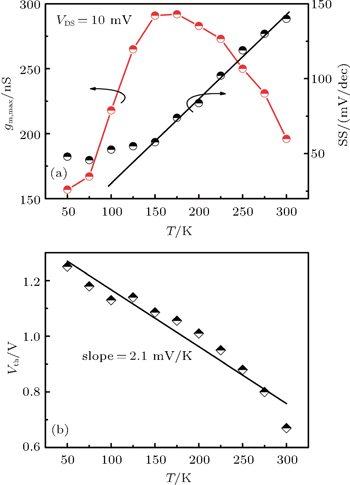
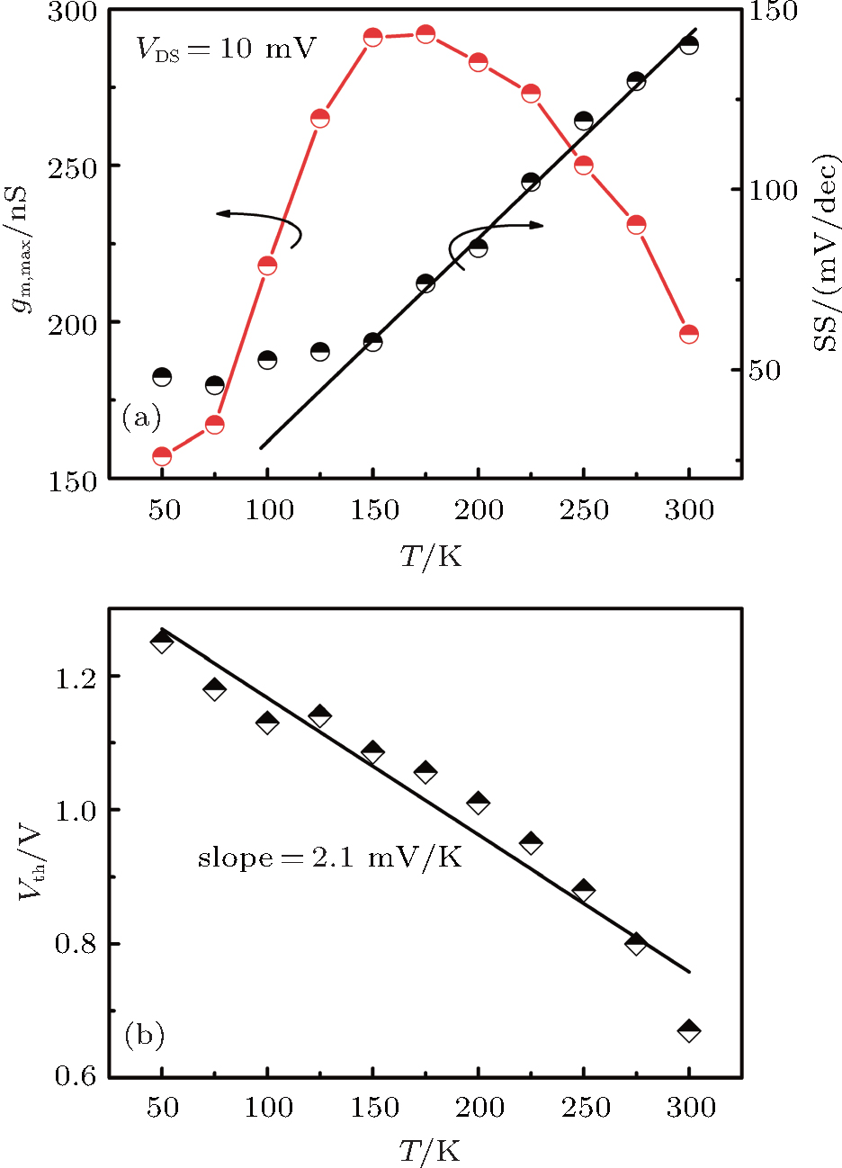
3.3. Temperature-dependent electrical parametersAny variation of temperature will induce the change of electrical parameters of JNT device, such as the threshold voltage, flatband voltage, subthreshold swing and electron mobility. Temperature instabilities of some electrical parameters are investigated in a temperature range from 50 K to 300 K.
The left curve of Fig. 5(a) shows the variation of maximum transconductance gm,max with temperature in the predicated value. Since gm,max is a measure of the peak effective mobility, the variation of gm,max with temperature reflects the variation of electron effective mobility with temperature. The measured result shows that the electron mobility increases in a temperature range from 50 K to 175 K, because impurity coulomb scattering is dominant in the scattering rate for the heavily doped channel at low temperatures. While the electron mobility decreases in a temperature range from 175 K to 300 K, which can be ascribed to the enhancement of phonon scattering at higher temperatures. Our data are in agreement with the reported results in Ref. [16]. The SS follows the theoretical expression SS = n(kBT/q)ln (10), where n is the body effect coefficient. The value of n equals 1 in the ideal condition. The right plot in Fig. 5(a) shows the temperature dependence of SS. It almost presents a linear decrease in a temperature range from 300 K to 150 K and the average value of n is 2.8, which stems from the existence of traps around Si/SiO2 interface and in the poly-silicon gate. However, the shift slope of SS with temperature becomes slightly smaller than the predicted value at temperatures lower than 100 K due to the nonuniform distribution of traps,[17] which is mainly induced by etching and thermal oxidation procedure.
Figure 5(b) shows the evolution of Vth with temperature. It can be seen that Vth is negatively shifted with temperature increasing. The experimental negative shift of Vth is 2.1 mV/K. From Ref. [18], the variation of Vth with temperature is expressed as
where
ni and
Nd denote intrinsic carrier density and the doping concentration, respectively. The theoretical value of d
Vth/d
T is 0.45 mV/K, which is much smaller than the experimental value of 2.1 mV/K. We attribute this phenomenon to the influence of thermal activation of traps.
[19,20] 4. ConclusionsIn this work, the JNT with the physical channel cross-section area of 28 nm×55 nm is fabricated by femtosecond laser lithography. The extracted low-field electron mobility is 290 cm2·V−1·s−1, inferring that this method can well impede the damage of the crystalline structure of silicon. Besides, the increase of current steps with gate voltage is clearly observed at a temperature of 10 K, which is attributed to the electron transport through degenerated 1D subbands formed in the nanowire. The mobility is phonon limited at temperatures larger than 175 K, while it appears to be limited by impurity scattering below that temperature. The slope of threshold voltage shift with the temperature is 2.1 mV/K due to the influence of interface traps. These results help us better understand the transport mechanism in JNT at low temperatures. The development of this novel maskless lithography has tremendous potential for opening a new market in nanoscale device fabrication. The low cost and high resolution process is expected to provide an accurate, repeatable and efficient means of creating nanoscale structures for device applications.


 , Wang Hao, Lyu Qi-feng, Zhang Wang, Yang Xiang, Yang Fu-Hua‡,