


Aberration-corrected scanning transmission electron microscopy for complex transition metal oxides
[Zhang Qing-Hua1, Xiao Dong-Dong2, Gu Lin2, 3, †,  ]
]
]
|
|


† Corresponding author. E-mail:
Project supported by the National Key Basic Research Project, China (Grant No. 2014CB921002), the Strategic Priority Research Program of Chinese Academy of Sciences (Grant No. XDB07030200), and the National Natural Science Foundation of China (Grant Nos. 51522212 and 51421002).
Lattice, charge, orbital, and spin are the four fundamental degrees of freedom in condensed matter, of which the interactive coupling derives tremendous novel physical phenomena, such as high-temperature superconductivity (high-Tc SC) and colossal magnetoresistance (CMR) in strongly correlated electronic system. Direct experimental observation of these freedoms is essential to understanding the structure-property relationship and the physics behind it, and also indispensable for designing new materials and devices. Scanning transmission electron microscopy (STEM) integrating multiple techniques of structure imaging and spectrum analysis, is a comprehensive platform for providing structural, chemical and electronic information of materials with a high spatial resolution. Benefiting from the development of aberration correctors, STEM has taken a big breakthrough towards sub-angstrom resolution in last decade and always steps forward to improve the capability of material characterization; many improvements have been achieved in recent years, thereby giving an in-depth insight into material research. Here, we present a brief review of the recent advances of STEM by some representative examples of perovskite transition metal oxides; atomic-scale mapping of ferroelectric polarization, octahedral distortions and rotations, valence state, coordination and spin ordering are presented. We expect that this brief introduction about the current capability of STEM could facilitate the understanding of the relationship between functional properties and these fundamental degrees of freedom in complex oxides.
Originally, scanning transmission electron microscopy (STEM) was invented in the 1930s as an alternative to light microscope to overcome the diffraction limit of visible light due to the short wavelengths of fast electrons. After efforts of generations of scientists and engineers, now STEM has evolved into a powerful comprehensive equipment for characterizing materials with a high spatial resolution and become indispensible in material research, far more than just a magnifier. In an STEM, fast electrons, emitted from the electron gun, are accelerated to several hundreds of kV and subsequently penetrate the thin sample, where electron beams interact strongly with materials (specimen) with a scattering cross section thousands of times bigger than that of x-ray, producing various types of signals, such as forward scattering electrons, backward scattered electron and characteristic x-ray, fluorescence, etc. Most of such signals have been collected and developed into a number of techniques capable of providing specific information about materials in different perspectives. Much information, such as real-space structure projection, reciprocal diffraction, composition, and electronic state, can be collected from the same local region of sample, allowing investigations of structure-property relationship with full perspectives.
As is well known, the realm of condensed matter physics is mostly governed by quantum mechanics, where electron correlations between atoms coded in a crystalline or an amorphous matrix determine various functional properties. To understand or simulate these correlations in theory, atom positions should be known accurately, because they determine the overlay of atomic potential and affect the electron configuration. Meanwhile, states of valence electrons including population, orbit and spin are also significant for determining electronic and magnetic behaviors of materials. It is desirable to obtain information about these four freedoms on an atomic scale to interpret novel properties and explore the physics mechanism behind. Half a century ago, physicist Feynman raised a challenge of “improving the resolution of the electron microscope by 100 times” to explore “the plenty room at the bottom”, considering the 10 angstrom resolution in his era. Thanks to the advent of aberration correctors, nowadays, a spatial resolution of 0.5 angstrom has been achieved in a well-made aberration-corrected STEM.[1] The resolution is no longer limited by aberration in magnetic lens, but hampered by the physical width of atom itself determined by the electrostatic potential and thermal motion of atom.[2] In 2011, H atom columns in a crystalline compound YH2 were successfully visualized by the angular bright-field (ABF) imaging technique[3] in an STEM, indicating that all members in the periodic table of elements can be resolved now. In addition, chemical analysis including composition and electron configuration, such as valence state, can also be performed simultaneously on an atomic scale, providing a multi-dimensional perspective on the natures and states of materials. Thus, concretely, what can STEM provide for the four freedoms with the atomic-scale capability?
Here, we will give a brief introduction of recent advances of aberration-corrected STEM in perovskite transition metal oxides (TMOs) by several representative examples. The unprecedented capability of aberration-corrected STEM in atomic-scale mapping of ferroelectric polarization, octahedral distortions and rotations, valence state, coordination and even spin ordering is demonstrated.
Prior to our introduction, some basic knowledge about STEM will be briefly introduced. We do not plan to explain imaging & spectrum theory or principle nor how to acquire different kinds of STEM data, instead, we will focus on what kinds of information each technique can provide for us, aiming to benefit non-micorscopist researchers in a quick and simple way. An STEM integrates imaging, diffraction and spectroscopy techniques, making itself as a powerful instrument for characterizing the physicochemical natures of various materials. These techniques provide different aspects of materials through collecting scattered electrons or emitted x-ray in corresponding collection geometry. Figure
 | Fig. 1. Schematic diagram of the common imaging and spectrum modes in an STEM, composed of annular dark-field (ADF) or high-angle annular dark-field (HAADF) images(depending on the inner angle β1), bright-field (BF) or angular bright-field (ABF) image (depending on the inner angle α0), electron energy-loss spectroscopy (EELS) and x-ray energy dispersive spectroscopy (EDX). |
When the inner angle of the detector is greater than the convergence angle of the probe, an angular dark-field (ADF) image can be recorded.[4] Specially, LAADF, MAADF, or HAADF images can be obtained, which are dependent on the inner angles: low, medium, and high angle, respectively. They provide complementary information about the material structure due to their respective contrast mechanisms. For example, LAADF image, in which coherent diffraction effects contribute a large part to the recorded signal, is good at visualizing the strained or defected features; HAADF image with an inner rather larger angle, mostly contributed by the Rutherford scattering of electron by the nuclei at a high angle, shows an approximate Z2 dependence of atom number, which is also named Z-contrast image (Z is the element number), providing a high explainability of atomic column over a large variation of thickness and defocus. MAADF image with a medium inner angle and outer angle can combine the advantages of both LAADF and HAADF imaging techniques, which can be tuned according to practical experimental requirements. It is powerful to image the heavy atoms in the materials due to their strong ability to scatter the incoming electrons. Of course, the situation in real samples may be a little more complex due to some effects which can make the scattering dependence different from that of isolated atoms. Thus, some imaging simulations are also needed for the sake of verification.
Recently, an angular bright-field (ABF) imaging technique has been developed for its sensitivity to the light elements, where the contrast of atomic columns is approximately proportional to the Z1/3. By ABF imaging, Okunishi et al.[5] impressed the world by the imaging O column in SrTiO3 and N column in Si3N4, which O and N were clearly visualized but invisible in the HAADF images. Findlay et al. further demonstrated the robust capability of ABF imaging in O column in SrTiO3 and TiO2 lattice and did lots of meaningful theoretical work for its contrast mechanism.[6–10] Lithium ion in LiV2O4 lattice was also directly imaged by Oshima et al.[11] Subsequently, imaging light elements, such as lithium and hydrogen, have occurred in extensive studies. More details about its origin and principle can be found elsewhere.[6,7]
Besides imaging the real-space structure by various imaging modes, electronic structure of material can also be investigated by the electron energy loss spectroscopy (EELS) equipped beneath electron microscope. It records the electron counts as a function of energy lost in the inelastic interactions between incoming electrons and specimen with a high efficiency, providing chemical bonding, valence, or coordination information, similar to x-ray absorption spectroscopy (XAS) but with a higher spatial resolution. Atomic scale EELS is invaluable in explaining the atomic structure of heterostructures. Nevertheless, EELS has a high background and limited energy range (usually below 2 keV); signals of some elements are difficult to extract from the background or acquire. As a complement, an energy-dispersive x-ray detector (EDX) sited at the upper position of column is used to collect the characteristic x-ray from the illuminated sample area, which is suitable for certain heavy elements. However, currently, the poor collection efficiency of EDX makes it very challenging to obtain a compositional map at the atomic resolution. Despite EELS and EDX both have some imperfections, combining with STEM, STEM-EELS and STEM-EDX have played an important role in characterizing the chemical and electronic structures of materials as demonstrated in the example shown later.
One of the benefits of aberration correction in the STEM is the elimination of the image delocalization caused by the lens aberrations. By using the drift correction procedures[12,13] and 2D Gaussian peak fitting,[14] now it is feasible to obtain the atom positions with a high accuracy (pm precision), allowing many applications in oxides materials. In addition, complementary HAADF and ABF images can be simultaneously acquired, thus, the positions of both heavy and light atom can be determined. Specifically, HAADF images record the cation positions with high accuracy, while ABF images show the oxygen columns, allowing the octahedral rotations to be measured. Here, we demonstrate two applications: ferroelectric mapping, and determining octahedral distortion and rotation.
Ferroelectric domain walls have recently been found to exhibit unique properties such as enhanced conductivity[15] and photocurrent generation.[16] In displacive ferroelectrics, the polarization is related to cationic or anionic shifts with respect to the symmetry center of the unit cell, therefore the polarization vector and domain wall can be determined by the imaging the atomic position. As mentioned above, HAADF imaging is dominated by Rutherford scattering of electron by the nuclei; image contrast of white spots usually appears exactly at the locations of the atomic columns, which lays the foundation for acquiring the atomic positions reasonably. Therefore, HAADF imaging has been applied to the ferroelectric domain investigation soon after the availability of the sub-angstrom probe. Benefiting from the efforts by the HRTEM community,[14] atomic positions can be located with picometre precision using 2D Gaussian peak fitting in the atomic resolution HAADF images.
By virtue of HAADF imaging, Zhang et al.[17] identified two types of interlocked domain walls in improper ferroelectric RMnO3 (R-rare earth); subsequently six-state and four-state vortex configurations of ferroelectric domains have also been revealed.[18,19] Through quantitatively extracting the atomic positions of Fe ions in BiFeO3, Nelson et al.[20] demonstrated the spontaneous vortex nanodomain arrays at ferroelectric heterointerfaces. By the phase-field simulation, the presence and absence of free charge carriers at the film/air interface and the film/substrate interface have been discussed. Further, Tang et al.[21] combined the HAADF imaging with polarization analysis to investigate the strained ferroelectric PbTiO3 film, and a periodic array of flux-closure quadrants has been revealed. By geometry phase analysis (GPA) on the atomic scale HAADF images, a large strain gradient up to 109 per meter in the vicinity of the core was visualized. More strikingly, by exploiting the competition among charge, orbital and lattice degrees of freedom in superlattices of alternating lead titanate and strontium titanate layers, the complex polar vortices have been recently realized in oxide superlattices by Yadav et al.[22] As shown in Fig.
 | Fig. 2. Observations of vortex–antivortex structures. Panel (a) displays the cross-sectional HR-STEM image with an overlay of the polar displacement vectors (PPDs, indicated by yellow arrows) for a (SrTiO3)10/(PbTiO3)10 superlattice, showing that an array of vortex–antivortex pairs is present in each PbTiO3 layer. Panel (b) shows a magnified image of a single vortex–antivortex pair, indicating the full density of data points (one for each atom) and the continuous rotation of the polarization state within such vortex–antivortex pairs. Panel (c) exhibits the curl of the polar displacement (∇ × PPD)[010] for the same vortex–antivortex pair, revealing the alternating rotation directions of the structures. The (∇ × PPD) [010] curl value is plotted with a red/blue colour scale where no-vorticity (curl = 0) is in white, clockwise (negative) is in blue and anticlockwise (positive) is in red. Panel (d) indicates polarization vectors from a phase-field simulation of the same (SrTiO3)10/(PbTiO3)10 superlattice, which predicts vortex–antivortex pairs that closely match the experimental observations. Reproduced from Ref. [22]. |
The ABO3 pervoskite is a simple and magic structure with rich functionalities which can contain a large variety of cations by distortions and rotations of BO6 octahedra. Changes in B–O–B bond length and bond angle can impose significant influences on the electronic and magnetic properties. Thus, charactering BO6 octahedral is vitally important for fully understanding fundamental aspects of materials. However, it is challenging to image the O columns due to weak scattering section of oxygen. Benefiting from the newly developed ABF imaging,[23] light elements such as O and Li can be visualized directly.[6–11] Borisevich et al.[24] combined the HAAAF and ABF images to quantify the cationic position and oxygen position respectively, the suppression of octahedral tilt has been visualized at the BiFeO3–La0.7Sr0.3MnO3 heterostructure interface. By combining with low-loss electron energy loss spectroscopy imaging, it was found that the La0.7Sr0.3MnO3 severely constrains the octahedral rotations in BiFeO3, which is the origin of the lattice expansion seen in the Z-contrast image, resulting in a dielectric anomaly as detected by EELS. Subsequently, a large number of investigations on the octahedral distortion by the ABF imaging in other ABO3 system have been conducted.[24–28] For example, Ryotaro et al.[29] revealed significant distortions of RuO6 and ScO6 octahedra at the heterointerface between a SrRuO3 film and a GdScO3 substrate; Sanchez-Santolino et al.[25] examined the oxygen octahedral distortions in LaMnO3/SrTiO3 superlattices; Qiao et al.[28] revealed symmetry-breaking induced the interfacial structure of CoO6 octahedral building-blocks, which results in expanded octahedron volume, reduced covalent screening, and stronger electron correlations in epitaxial LaCoO3/SrTiO3 heterostructures. Further, Lunkenbein et al.[27] obtained the distribution of oxidation states in the cation columns at different sites of a complex molybdenum vanadium mixed oxide by the direct imaging of octahedral distortion. These researches adequately exhibited the robust imaging capability for oxygen, which provided invaluable clues to the investigation of heterostructure and oxides.
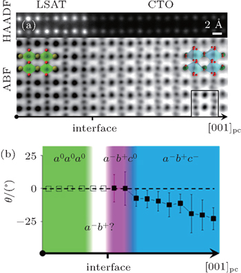
Recently, the recognition that resulting distorted shape of the atom column projections can provide additional information has been realized. Borisevich et al.[30] applied principal component analysis (PCA) of atomic column shapes in HAADF images, revealing polarization and octahedral tilt behavior across uncharged and charged domain walls in BiFeO3. Subsequently, ABF image simulations by He et al.[26] showed that qualitative and quantitative information about BO6 rotation in three-dimensional (3D) can be obtained. They proposed a new method of using oxygen column shape analysis of ABF images in specific orientation to map the 3D octahedron rotation in perovskite heterointerfaces as demonstrated in La0.7Sr0.3MnO3 (LSMO)/Eu0.7Sr0.3MnO3(ESMO) superlattice and CaTiO3 (CTO)/(LaAlO3)0.3(Sr2AlTaO6)0.7 (LSAT) interface. It was found that the ESMO/LSMO interface exhibits an abrupt change between two symmetries; while CTO/LSAT interface involves an extensive interfacial layer with a distinct BO6 rotation pattern. Figure
 | Fig. 3. Interface of the CTO film and the LSAT substrate with a transition layer of a different BO6 rotation pattern. Panel (a) shows the STEM HAADF and ABF images of the CTO/LSAT interface along [110]pc axis, with overlapped polyhedral model and one simulated ABF image (inset). The [001]pc direction for both oxides is the out-of-plane direction, which is the film growth direction. Panel (b) displays the averaged profile of θ. θ is an inclination angle between the major axis of the contrast ellipse of oxygen and horizontal La–La direction. The solid squares refer to measured values, and the empty squares represent the speculated values for the LSAT substrate, where there is no well-defined deviation from roundness to detect. Symmetries of BO6 rotation across the interfaces are displayed in overlaid colors (green, a0a0a0; white, a−b+?; purple, a− b+c0; blue −a− b+c−), which are determined from θ angle measurement as well as other analysis, such as PCA (see text and Supporting Information). In contrast to the case of the LSMO/ESMO interface, a different BO6 rotation pattern (purple, a−b+c0) is found in the transitional layer at the interface. Reproduced from Ref. [26]. |
The physical properties of TMOs are intimately related to the occupancies of the partially filled 3d bands, which are strongly hybridized with the O 2p bands and determine their oxidation states. Compared with reciprocal spectroscopic techniques probing unoccupied density of states (DOS) around the Fermi level, EELS in the STEM is suitable for imaging chemical compositions and electronic properties in real space with atomic resolution.[31] In addition, electron energy-loss near-edge structure (ELNES) can also be used to detect bonding states such as the transition-metal oxidation states. Both the transition metal L edge and the O K edge provide a direct insight into the electronic structure, where the L3 and L2 edges correspond to the transitions from 2p3/2 to 3d3/2/3d5/2 and from 2p1/2 to 3d3/2 of TM ions, respectively; the O K edge corresponds to the transition from 1s to hybridized 2p band.[32] After successfully implementation of aberration correctors in the STEM equipped with a cold-field gun in recent years, a sub-angstrom probe with high current makes the atomic resolved EELS with improved signal-noise ratio truly feasible in routine practice.[33] Finally, the direct simultaneous probing of the structure, chemistry, and electronic properties of materials with atomic resolution becomes routinely attainable.
In resolving the atomic structure of oxide interface, EELS is invaluable for distinguishing interface termination in cases where elements are difficult to distinguish by HAADF images due to the nearly equal atomic number Z. Early in 2008, with a fifth-order aberration-corrected STEM which provides a factor of 100 increase in signal over an uncorrected instrument, Muller et al.[33] demonstrated 2D elemental and valence-sensitive imaging at atomic resolution by STEM-EELS within less than a minute. La, Ti, and Mn columns in an La0.7Sr0.3MnO3/SrTiO3 multilayer were clearly identified, whereas it is not easy to distinguish between Ti and Mn in HAADF image due to their small Z difference.
Besides elemental imaging, ELNES of EELS can provide rich information about electronic structures of materials. Especially in perovskite-structured TMOs, some common features in the ELNES can be recognized because of similar coordination, Jahn–Teller splitting, and 3d degeneracy of BO6 octahedron, which provides us with a general guide to the analysis of the ELNES. For example, valence states of TM (Mn) ions have a linear correlation with the energy difference between pre-peak and main peak in O K edges, L2,3 ratio of TM L edges and the chemical shift of L edges in ABO3 (LaxCa1−xMnO3).[34]
Nowadays, combining a cold field-emission gun with aberration corrector, a sub-angstrom probe with high brightness enables the atomic resolved EELS with adequate signal-noise ratio to visualize the fine structure of O K edge and TM L edges; an upsurge of atomic resolved EELS has already come.[35–45] By fitting the ELNES of Mn L2,3 edges of Mn3O4, a 2D mapping of Mn2+ and Mn3+ has been obtained in the spectrum imaging by Tan et al.,[35] shedding light on the charge-ordered materials such as LuFeO4 and PrxCa1−xMnO3. When turning to heterointerfaces or supperlattices, atomic resolved EELS has played a powerful role in characterizing the electrostatic screening, polar behavior, interface magnetism,[43] charge transfer,[44,46] etc.
Kim et al.[41] applied combined atomic resolved HAADF image and STEM-EELS to the BiFeO3/LaxSr1−xMnO3 interface and found an oxygen-vacancy screening evidenced by unexpected lattice expansion, anomalous decrease of the Mn valence, and the change in oxygen K-edge intensity at the negative polarization charged interface while a purely electronic screening has insignificant changes in lattice and electronic property at the surface with positive polarization charge. Using similar imaging techniques, oxygen-vacancy-induced polar layer in a superlattice comprised of two nonpolar oxides (LaFeO3)2/(SrFeO3) was revealed by Mishra et al.,[42] where diffusions of La, Fe, and O, and valence state of Fe were mapped out unit by unit. Figure
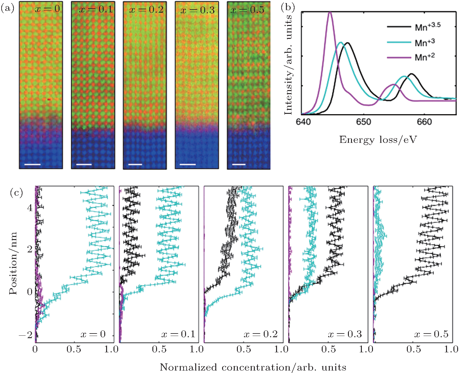 | Fig. 4. (a) Mn valence changes at the series of La1−xSrxMnO3/SrTiO3 interfaces. Spectroscopic images are shown for x = 0, 0.1, 0.2, 0.3, and 0.5 films (from left to right), where Ti is plotted in blue, Mn in green, and La in red, and the x = 0.5 image shows cation ordering not observed in other films. (b) Three Mn reference spectra for Mn+2, Mn+3, and Mn+3.5, used to determine the Mn valence across the interface. (c) The results of the non-negative non-linear least squares fit of the components in panel (b) for x = 0, 0.1, 0.2, 0.3, and 0.5 (from left to right). Error bars plot the standard error of the mean generated from five binned regions from each spectroscopic image. Scale bar is 1 nm. Reproduced from Ref. [46]. |
Beyond valence states and charge analysis by the L edges of TM ions, the ELNES of O K edges also carries much information about electronic properties of the TM–O bonding, coordination environment, hybridization state, spin state, etc. We find that ab-initio simulation is also vitally important and indispensable in understanding these atomic-level ELNESs of O K edges, providing a novel insight into the electronic behaviors. Mundy et al.[36] performed a 2D analysis of oxygen local bonding environments for the fine structure of the O K edge; two distinct signals for the two inequivalent oxygen sites were identified in multiferroic LuFe2O4, which can be attributed to the different hybridizations of the O p orbitals to the Lu and Fe d orbitals as suggested by ab-initio simulation. Haruta et al.[38] made a detailed atomic resolution chemical bond analysis of ELNES of O K edges of La2CuO4 and observed anisotropic chemical bonding of the oxygen 2p state with the Cu 3d, 4p states and La 5d/4f states. Strong dependence of effect of core-hole in the O K-edge on the nature of the local chemical bonding was also verified by first-principles band structure calculations.
Specifically, in brownmillerite Ca2FeCoO5 consisting of repetitive octahedral and tetrahedral coordination layers, Fe and Co both have a constant valency 3+ but different coordinations, making it an ideal candidate to demonstrate pure coordination mapping at atomic resolution. Turner et al.[37] demonstrated a coordination mapping in brownmillerite Ca2FeCoO5 as shown in Fig.
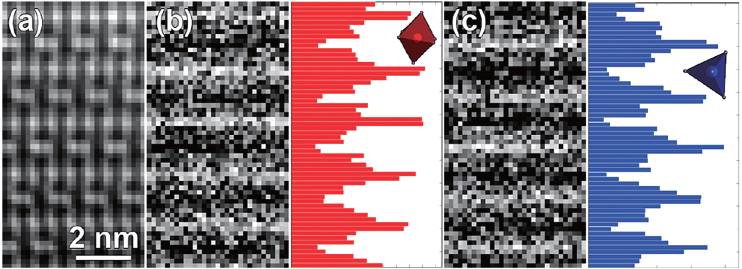 | Fig. 5. Octahedral and tetrahedral EELS maps generated by fitting the average components to the atomic resolution data (a), the octahedral component (b) and tetrahedral component (c) peak at the corresponding Fe/Co intermixed layers, as clearly evidenced by the intensity profiles over the full image width. Reproduced from Ref. [37]. |
In addition, the pre-peak of O K edge can also reflect the spin state of Co atoms in perovskite cobalts. It has been found in LaCoO3 that changes in the net spin of Co may have a fingerprint in the ELNES of O K edges, where the higher pre-peak intensity corresponds to the lower spin state; meanwhile the Co oxidation state does not change indicated by the constant Co L2,3 ratio.[47] As shown in Fig.
 | Fig. 6. (a) Averaged O K and Co L2,3 spectra from the bright stripe (red) and dark stripe (blue), scaled for presentation purposes. (b) Superstructure at higher magnification. Inset: area used for spectrum imaging along with the O K image (false color) generated by integrating PCA-treated spectra over a 30-eV window, after background subtraction. The acquisition time is 1.5 s per pixel. (c) Simulated O K edges for the O3 (red) and O1 (blue) atoms for the La0.5Sr0.5CoO2.25 compound (top) along with the Co 3d PDOS for Co1 (blue) and Co2 (red) (bottom). Reproduced from Ref. [48]. |
It is shown that aberration-corrected STEM provides an unprecedented tool for characterizing structures and electronic structures of perovskite oxides on an atomic scale, including real-space structure determination with picometer precision, spectroscopic detection of composition, local bonding, coordination, and even spin ordering, assisted by theory simulations. Besides perovskite oxides, atomic resolved STEM-HAADF and STEM-EELS play a similar invaluable and indispensible role in characterizing other material systems such as lithium-ion imaging in rechargeable batteries. At present, it becomes a routine tool for material scientists to resort STEM to find the microscopic origin of novel properties, which leads to an in-depth insight into existing materials and the design of new material with desired properties. It can be recognized that the future development of materials will be critically dependent on the application and further development of aberration-corrected STEM. With fifth-order aberrations or more advanced correctors, mapping minor structural distortions, orbitals and electronic properties around impurities, defects, and interfaces can be expected.
| 1 | |
| 2 | |
| 3 | |
| 4 | |
| 5 | |
| 6 | |
| 7 | |
| 8 | |
| 9 | |
| 10 | |
| 11 | |
| 12 | |
| 13 | |
| 14 | |
| 15 | |
| 16 | |
| 17 | |
| 18 | |
| 19 | |
| 20 | |
| 21 | |
| 22 | |
| 23 | |
| 24 | |
| 25 | |
| 26 | |
| 27 | |
| 28 | |
| 29 | |
| 30 | |
| 31 | |
| 32 | |
| 33 | |
| 34 | |
| 35 | |
| 36 | |
| 37 | |
| 38 | |
| 39 | |
| 40 | |
| 41 | |
| 42 | |
| 43 | |
| 44 | |
| 45 | |
| 46 | |
| 47 | |
| 48 | |
| 49 |