1. IntroductionUsing a mature technique to synthesize the same material with different morphologies and grain sizes, scientists are able to accurately control the properties of materials through changing the experimental conditions.[1–4] Different morphologies or grain sizes may differ in both chemical and physical properties even for the same sample with the same structure, which is due to the different arrangements of surface atoms and the ratio of the number of atoms on the surface to that in the bulk of nano-/micro-structured crystals, corresponding to the ratio of the surface energy and the cohesive energy.[4–6]
Pressure can induce direct and significant changes in atomic and electronic structure, and allows the tuning of the properties. In some earlier publications, the size effects in ZnS,[7] ZnO,[8] AlN,[8] Y2O3,[9] etc. under high pressure have been reported. These reports showed that the sample properties under high pressure are highly dependent on the initial grain size synthesized by the chemical method. The synthesis- and pressure-induced interfaces are named the chemical interface and physical interfaces, respectively. Since 2010, Wu et al. have reported that stress-induced silver nanoparticles turn into one-dimensional (1D)-nanostructure arrays,[10] a pressure-driven sintering of spherical nanoparticle arrays into nanostructured gold architectures,[11] and a pressure-induced silver nanoparticle super-lattice into mechanically stable nanowires.[12] Since 2012, the pressure-induced surface nanocrystallizations in Cu2O,[13] Alq3,[14] and Zn2SnO4 have been reported.[15] All the reported results in these two groups indicate that the pressure-induced physical interfaces affect the mechanical, optical, and electrical transportation properties, the phase sequence, transition pressure, etc.
As is well known, it is difficult to characterize the surface or interface properties directly under high pressure due to experimental restrictions. The researchers investigated the surface and interface properties by an indirect method through combining the SEM or TEM with the in situ optical measurements and in situ electrical transportation methods. To the best of our knowledge, there have been no in situ experimental data available under high pressure for the primitive samples with different surfaces and interfaces formed by the physical forces. Considering the different influences of chemical interfaces and physical interfaces, it will thus be valuable to conduct high pressure in situ experiments on the samples with different physical interfaces. The grind method is used to generate samples with different average grain sizes.
As a typical II–VI group semiconductor, Zinc selenide (ZnSe) has several potential applications and has been widely studied.[16–20] It was found that ZnSe has size-dependent optical and morphological properties,[21,22] and under compression the ZnSe transforms from zinc blende to cinnabar-type structure and then to rock salt structure.[23–27] Owing to the crystal size reduction, Campos et al. observed an increase of the phase-transition pressure.[28] However, it is not clear how the grain boundary changes and affects the electrical property of ZnSe particles under high pressure. In this paper, two ZnSe samples with different particle sizes obtained by the grind method and their grain boundary behaviors under high pressure are studied by in situ alternating the current (AC) impedance method.
2. ExperimentThe ZnSe sample with a purity of 99.999% was bought from Alfa Aesar Co. To obtain a different average size, the sample was ground manually by using an agate mortar. A Zetasizer nano series particle size analyzer was used to measure the particle size. Two samples with average sizes of 859 nm and 478 nm were obtained after one-and-two-hour grinding, respectively. In situ AC impedance spectrum measurements under high pressure with a two-electrode configuration microcircuit were performed in a diamond anvil cell (DAC) with an anvil culet of 400 μm in diameter. A T301 stainless steel gasket served as one electrode and a thin-film electrode integrated onto one diamond anvil surface served as another electrode.[29] More details about the microcircuit fabrication and the insulation between the gasket and the film electrode have been previously described.[30,31] The pressure was determined by the pressure induced shift of the R1 ruby fluorescence line.[32] No pressure medium was used to assure that the impedance spectrum reflects the information of the pure ZnSe samples. The AC impedance spectra were measured with a Solartron 1260 impedance analyzer equipped with a Solartron 1296 dielectric interface. An AC sine voltage signal with an amplitude of 1 V and a range from 0.01 Hz to 10 MHz was applied to the samples.
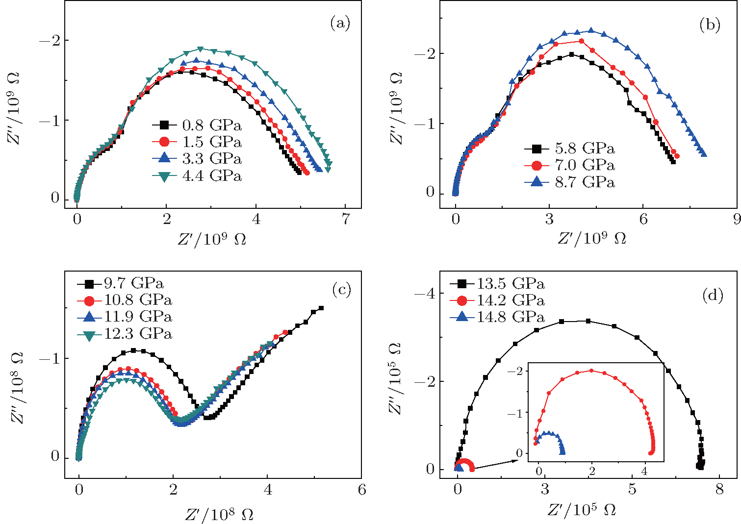
3. Results and discussionThe impedance data of the ZnSe sample with a grain size of about 478 nm at different pressures are presented in Fig. 1. In a pressure range from ambient pressure to 8.7 GPa, the impedance spectrum is composed of two overlapping semicircles, the arcs at the high frequency area on the left-hand side represent the contribution of the bulk, and the arcs at the low frequency on the right-hand side describe the boundary contribution as shown in Figs. 1(a) and 1(b). Through the comparison, we find that the arcs corresponding to the bulk contribution are much weaker than those of the boundary contribution, which illustrates the boundary conduction dominates the electrical transport behavior of ZnSe in this pressure range. In most cases, the resistances of II–VI semiconductors decrease with increasing pressure.[33,34] However, we surprisingly find that the resistance of ZnSe gradually increases with increasing pressure. This can be explained by the fact that the band gap of ZnSe is predicted to gradually increase with increasing pressure. The result agrees well with the theoretical calculation of Durandurdu[35] and the lowest direct absorption edge experiment result of Ves et al.[36]
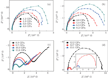
As shown in Fig. 1(c), when the pressure increases up to 9.7 GPa, both the impedance shape and its changing trend of ZnSe change. The impedance is composed of a semicircle in the high frequency area and an up-inclined arc in the low frequency area, which represents bulk conduction and the exhausting of the carrier in grain boundary,[37] respectively. Above 9.7 GPa, the resistance of ZnSe decreases with increasing pressure. Theoretical calculations reported the existence of a narrow field of stability (10.2 GPa–13.4 GPa) for a four-fold coordinated cinnabar-type phase,[25] so the changes of the impedance spectrum from 9.7 GPa to 12.3 GPa can be attributed to the phase transition of ZnSe.
When the pressure rises to 13.5 GPa, the impedance spectrum transforms into only one semicircle representing the boundary conduction as depicted in Fig. 1(d). The value of bulk resistance is very low and emerged in the figure. Above 13.5 GPa, the cinnabar-type phase of ZnSe transforms into rock salt phases,[38–40] which belongs to the metallic phase, resulting in the sharply reducing boundary resistance.
The impedance data of the ZnSe sample with a grain size of 859 nm at different pressures are shown in Fig. 2. In a pressure range of 0 GPa–8.2 GPa (as shown in Figs. 2(a) and 2(b), the impedance spectra are only one), the semicircle represents the bulk conduction. This can be explained by the fact that the boundary resistance value of the ZnSe sample with a grain size of about 859 nm is very large, the responsive time constant is also large, and the characteristic frequency is lower than the low-range frequency of the measuring instrument, therefore, we cannot observe the semicircle representing the boundary conduction at the low frequency. In this pressure range, the resistance of 859-nm ZnSe gradually increases with increasing pressure, resulting from the band gap broadening in accordance with 478-nm ZnSe.
When pressure is higher than 8.9 GPa (as shown in Fig. 2(c)), the impedance of 859-nm ZnSe transforms into a semicircle with an up-inclined arc, and the resistance decreases with increasing pressure. The change trend is similar to that of 478-nm ZnSe above 9.7 GPa, but the transition pressure point is reduced by 0.8 GPa. Here, the size effect plays a key role in this physical phenomenon. A smaller grain size sample has a bigger surface/volume ratio and more interfaces under the condition of equal volume, so that the transition of the sample with smaller grain size needs higher energy to conquer the barrier formed by the surface energy and the cohesive energy. Therefore, the sample with a smaller grain size undergoes the phase transition at higher pressures.
Above 12.2 GPa (as shown in Fig. 2(d)), the impedance spectrum of the 859-nm ZnSe sample is similar to that of the 479-nm ZnSe sample in a pressure range of 13.5 GPa–14.8 GPa. The cinnabar-type phase of ZnSe transforms into the rock salt phase, resulting in the sharply reducing boundary resistance.
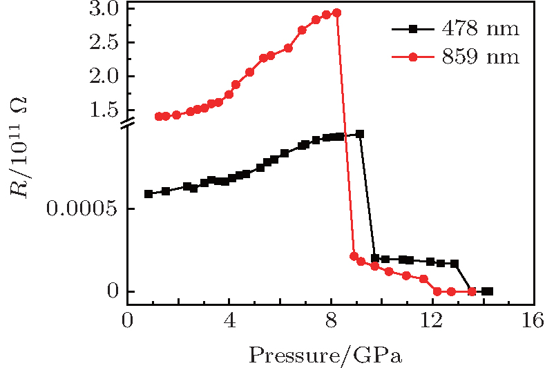
By comparing the impedance spectrum of 478 nm and that of the 859-nm ZnSe sample, we find that (i) the change trends of electrical properties of two specimens are consistent, and they undergo the same phase transition pathway from zinc blende to the cinnabar-type phase and then to the rock salt phase; (ii) the smaller grain size sample needs higher pressure points of structural phase transition; (iii) the boundary conduction plays a dominant role in the transportation process under high pressure. In order to observe the change of the grain boundary in a more intuitive manner, we obtain the resistance of the grain boundary by fitting the impedance spectra of two specimens, the results for the corresponding resistance are plotted in Fig. 3.
Figure 3 shows that the variation trends of the grain boundary resistance of two different particle size ZnSe samples. It can be seen that two curves are consistent with the change of the impedance spectrum. This suggests that the grain boundary resistance dominates the total resistance of ZnSe. By comparing the impedance spectra of two different particle size ZnSe samples at high pressures, we can see that the resistance of the 478-nm sample is smaller than that of the 859-nm sample. This is in sharp contrast to the universal law that the smaller the grain size, the bigger the resistance is. This is because the sample is obtained by mechanical grinding, the interface of the sample is different from the interface formed under the chemical condition. In the mechanical grinding process of ZnSe, a lot of defects are generated in both bulk and grain boundaries. The defect level in the band gap makes the electron excited from the highest occupied valence band to the lowest unoccupied conduction band easier, which will participate in the conduction process. Therefore, the sample resistance of 478 nm is smaller than that of 859 nm.
As the pressure is increased, the grain boundary resistances of the two samples decrease sharply. This is due to the structure phase transition of the sample from zinc blende to cinnabar phase structure. The grain boundary resistance decreasing interval (between 8.0 GPa–10.0 GPa) of the 859-nm ZnSe sample has a 0.8-GPa hysteresis compared with that of sample 478 nm. This is because the smaller the grain size, the higher the phase transformation pressure point is. After structural phase transition, the resistances of the two samples are equal to about 2.0×10⁸ Ω. Simultaneously, the carriers in the grain boundary are located in the charge depletion layer, which will not participate in the conduction process of the defect level. In a pressure range of 10.0 GPa–14.0 GPa, the grain boundary resistance of ZnSe decreases obviously, which is attributed to the structure transformation from cinnabar phase to rock salt structure followed by the grain boundary resistance decline in this pressure range.
4. Conclusions and perspectivesBy AC impedance spectrum measurements of different sizes of ZnSe samples under pressure, we find that the phase transition pathways of ZnSe with different particle sizes are the same, which transforms from sphalerite to cinnabar and then to the salt mine structure. However, the phase transition pressure point of the small size sample is higher than that of the big size one. This result can explain the difference between the transition pressure of cinnabar reported by Kobayashi et al. and that by Pellicer–Porres et al. The analysis of the fitting results of the grain boundary resistance indicates that the grain boundary resistance plays a leading role in the changing of the electrical properties caused by the phase transition. By comparing the impedance spectra of two different particle size ZnSe samples at high pressures, we find that the resistance of the 478-nm ZnSe sample is less than that of 859 nm. This phenomenon is in contrast to the universal law that the smaller the sample size, the greater the resistance is. This is because the interface of the sample treated by physical grinding has more defects than the chemical interface sample. The defect energy level makes the electron excited from the highest occupied valence band to the lowest unoccupied conduction band easier. As a result, more carriers will participate in the conduction process. If the particle size of the sample is smaller, there would be more defects, and the resistance of the grain boundary would be smaller. Therefore, when studying the electrical properties of a power sample, one should consider not only the scale effect but also the interface type.


 , Liu Cai-Long2, ‡,