Peng Ying-Zi, Song Yang, Xie Xiao-Qiang, Li Yuan, Qian Zheng-Hong, Bai Ru. Characterization of atomic-layer MoS2 synthesized using a hot filament chemical vapor deposition method. Chinese Physics B, 2016, 25(5): 058104
Permissions
Characterization of atomic-layer MoS2 synthesized using a hot filament chemical vapor deposition method
Peng Ying-Zi1, 2, †, , Song Yang1, Xie Xiao-Qiang1, Li Yuan1, 2, Qian Zheng-Hong2, Bai Ru2
Department of Physics, School of Science, Hangzhou Dianzi University, Hangzhou 310018, China
Center for Integrated Spintronic Devices, Hangzhou Dianzi University, Hangzhou 310018, China
Project supported by the Natural Science Foundation of Zhejiang Province, China (Grant Nos. LY16F040003 and LY16A040007) and the National Natural Science Foundation of China (Grant Nos. 51401069 and 11574067).
Abstract
Abstract
Atomic-layer MoS2 ultrathin films are synthesized using a hot filament chemical vapor deposition method. A combination of atomic force microscopy (AFM), x-ray diffraction (XRD), high-resolution transition electron microscopy (HRTEM), photoluminescence (PL), and x-ray photoelectron spectroscopy (XPS) characterization methods is applied to investigate the crystal structures, valence states, and compositions of the ultrathin film areas. The nucleation particles show irregular morphology, while for a larger size somewhere, the films are granular and the grains have a triangle shape. The films grow in a preferred orientation (002). The HRTEM images present the graphene-like structure of stacked layers with low density of stacking fault, and the interlayer distance of plane is measured to be about 0.63 nm. It shows a clear quasi-honeycomb-like structure and 6-fold coordination symmetry. Room-temperature PL spectra for the atomic layer MoS2 under the condition of right and left circular light show that for both cases, the A1 and B1 direct excitonic transitions can be observed. In the meantime, valley polarization resolved PL spectra are obtained. XPS measurements provide high-purity samples aside from some contaminations from the air, and confirm the presence of pure MoS2. The stoichiometric mole ratio of S/Mo is about 2.0–2.1, suggesting that sulfur is abundant rather than deficient in the atomic layer MoS2 under our experimental conditions.
A two-dimensional (2D) transition metal dichalcogenide (TMD) MX2, with M being a transition metal Mo or W, and X being a chalcogen, say S or Se, is attracting increasing interest for its great potential applications in the fields of nanoelectronics, optoelectronics, lithium batteries, hydrogen storage, and catalysis based on their novel nanoelectronic and optoelectronic properties.[1–3] In particular, 2D atomic MS2 ultrathin films were reported to have direct bandgaps of 1–2 eV and indirect-to-direct bandgap transition with reducing number of layers, leading to exotic electronic and optical properties.[4] Recently, it was proposed as a suitable material for valleytronics. Excitons and charged excitons (trions) can be created in TMD monolayers by optical excitation, as the use of circular polarized light was shown to produce long-lived valley polarization.[4–6] The strong emission from the direct gap structure of monolayer MoS2 also promises the applications in optoelectronics.[1]
TMD MoS2 materials have been known to be in the form of nested fullerene-like structure, consisting of a single layer of molybdenum atoms sandwiched between two layers of sulfur atoms in a trigonal prismatic structure.[7] Substantial efforts have been made to prepare layered MoS2 (extended to WS2),[8,9] such as scotch tape based micromechanical exfoliation, liquid exfoliation, physical vapor deposition, hydrothermal synthesis, thermolysis of single precursor containing Mo and S, chemical vapor deposition using MoCl2 or MoO3 and S as sources, laser-based thinning, plasma thinning and grapheme-assisted growth, where chemical vapor deposition (CVD) method is regarded as the most practical method of synthesizing large-area MoS2 nanosheets.[1] Large-area MoS2 films were synthesized on SiO2/Si substrates with CVD, using the sulfurization of MoO3 in the sulfur vapor assisted by the pretreatment for the substrates in a nitrogen environment.[1] In Ref. [10], a process for synthesizing the WS2 nanosheets through the sulfurization of an atomic layer deposition (ALD) WO3 film was described, which has systematic layer controllability and wafer-level uniformity. The limitations of previously reported methods were also mentioned in Ref. [10], such as difficulties in systematically controlling the thickness. With the help of the ability to control the thickness of the films more directly, highly homogenous TMD (MoS2) films were deposited on a large area by sulfurizing the pre-deposited thin Mo films.[11] Two steps after the thin film of Mo deposited were needed.[11] To our knowledge, it is still a challenge to synthesize the MoS2 ultrathin films in atomic layer with controllable thickness by using fewer processing steps.
Inspired by the reported successful research works, we adopt a simple hot filament chemical vapor deposition method by only one step to synthesize the MoS2 ultrathin films. The scale of millimeter square atomic-layer MoS2 films have been obtained, which has been confirmed by a thickness mapping measurement in our previous report.[12] In this paper, further investigations on the crystal structures, valence states, and compositions of the materials localized at an atomic layer area are carried out in order to confirm the production of the atomic layer MoS2. Regarding the future studies on the atomic layer MoS2, it is very important to investigate the preparation method in detail, because there may be something different in structure or composition among such thin layers obtained with different preparation methods.
2. Experiment
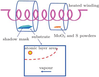
MoO3 and S powders mixed in a specific ratio were used as the reactants, in which MoS2 atomic layer can grow directly on substrates in one step by a hot filament chemical vapor deposition method. The reaction was done in a 30-mm-diameter horizontal quartz tube in vacuum. Specifically, a mixture of molybdenum trioxide (AR, 99.95%, Aladdin) and sulfur sublimed (Yongda) with a specific mole ratio of 1:49 (normally 0.003 g) was placed in the center of the tube as source. SiO2/Si(001) substrates were placed in another quartz tube near the heated winding downstream 2 cm away from the source material as the deposition acceptors. Before reaction began, the Si (001) substrates had been cleaned by the aqueous method and dried at 50 °C for half an hour. While deposition, the tube chamber was pumped into vacuum with a pressure lower than 0.1 kPa and flushed by Ar gas three times to remove the oxygen residue. Then, the winding was heated for deposition under 7 V bias condition for 90 s for growth. Finally, the tube was cooled down to room temperature for 30 min in vacuum. Figure 1 schematically illustrates the experimental setup.
Fig. 1. Schematic diagram of the experimental setup.
Microscopic and spectroscopic measurements aim to discover the structures, valence states, and concentration of the atomic layers MoS2. Tapping mode atomic force microscopy (AFM) experiments were performed in a multimode AFM microscope coupled to a micronano ChinaSPM controller (digital instruments). Commercially etched silicon tips with a typical resonance frequency of about 16 kHz were used as AFM probes. The crystal structures of the specimen were identified by x-ray diffraction (XRD) (DX-2500/2600) using CuKα radiation (λ = 0.1541 nm). Detailed lattice structures were obtained by a high-resolution transition electron microscopy (HRTEM) (Tecnai G2 F30) with an energy dispersive x-ray (EDAX) analyzer (DPP-II). In order to prepare the HRTEM specimen, the surface of ultrathin film was scratched by the TEM grids directly. In addition, the samples were characterized by transmission electron microscopy energy dispersive x-ray spectroscopy (TEM-EDX) to confirm whether the real stoichiometry meets the expectation. XPS (ESCALAB 250) was used to assess the chemical states of the thin films. All XPS spectra were corrected using the C 1s line at 284.6 eV. Photoluminescence (PL) spectra were measured with laser, which was operated at 405 nm wavelength, 5 mW power, and a large laser spot. We performed experimentally circularly polarized photoluminescence measurements on the atomic layer MoS2 and acquired circularly polarized PL spectra under the condition of right and left circularly polarized lights at room temperature in the case of off-resonance excitation state.
3. Results and discussion
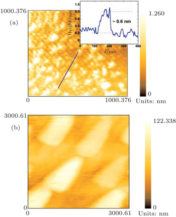
In order to show the specific features of the atomic layer MoS2 at the nucleation stage, the image of nucleation particles and the corresponding height profiles along a marked direction are shown in Fig. 2(a). The granular grains can be observed clearly, with a granular grain size of about 100 nm. From the image, the grain height is about 0.6 nm, which coincides with the typical grain height for monolayer MoS2. It is believed that ∼ 0.6 nm is the smallest monolayer nucleation grain size corresponding to the earliest stages of MoS2 growth, which sulfurized MoS2 sufficiently, and the small particles will be expanded and enlarged laterally as Mo and S species diffuse toward the expanding grains. In this stage, the nucleation particles show irregular morphologies under our experimental conditions. Figure 2(b) shows the AFM image of the MoS2 film at another spot (thicker spot). It can be seen that the film was granular and the grains are triangle shape. In Ref. [13], the authors discussed some possible stable edge structures for MoS2 quantum dots corresponding to different chemical potentials of sulfur based on the first principles calculations. Based on their studies, edge formation energy of the structure of Mo edge with S coverage is smaller than those of other structures in Ref. [13]. When the condition is S-rich, the most stable structure with the lowest energy is the structure of triangle quantum dot with Mo edge with S coverage. It is noted that the author declared that the above result is credible on the condition that the size is large enough. As the mole ratio of sulfur to molybdenum is 49:1 in our case, we suppose that the grains in the triangle shape are probably related to the high mole ratio of sulfur used in our preparations.
Fig. 2. AFM images and the corresponding height profiles (insets) along the marked directions of the ultrathin films, in the nucleation area (a) and another area (b), respectively.
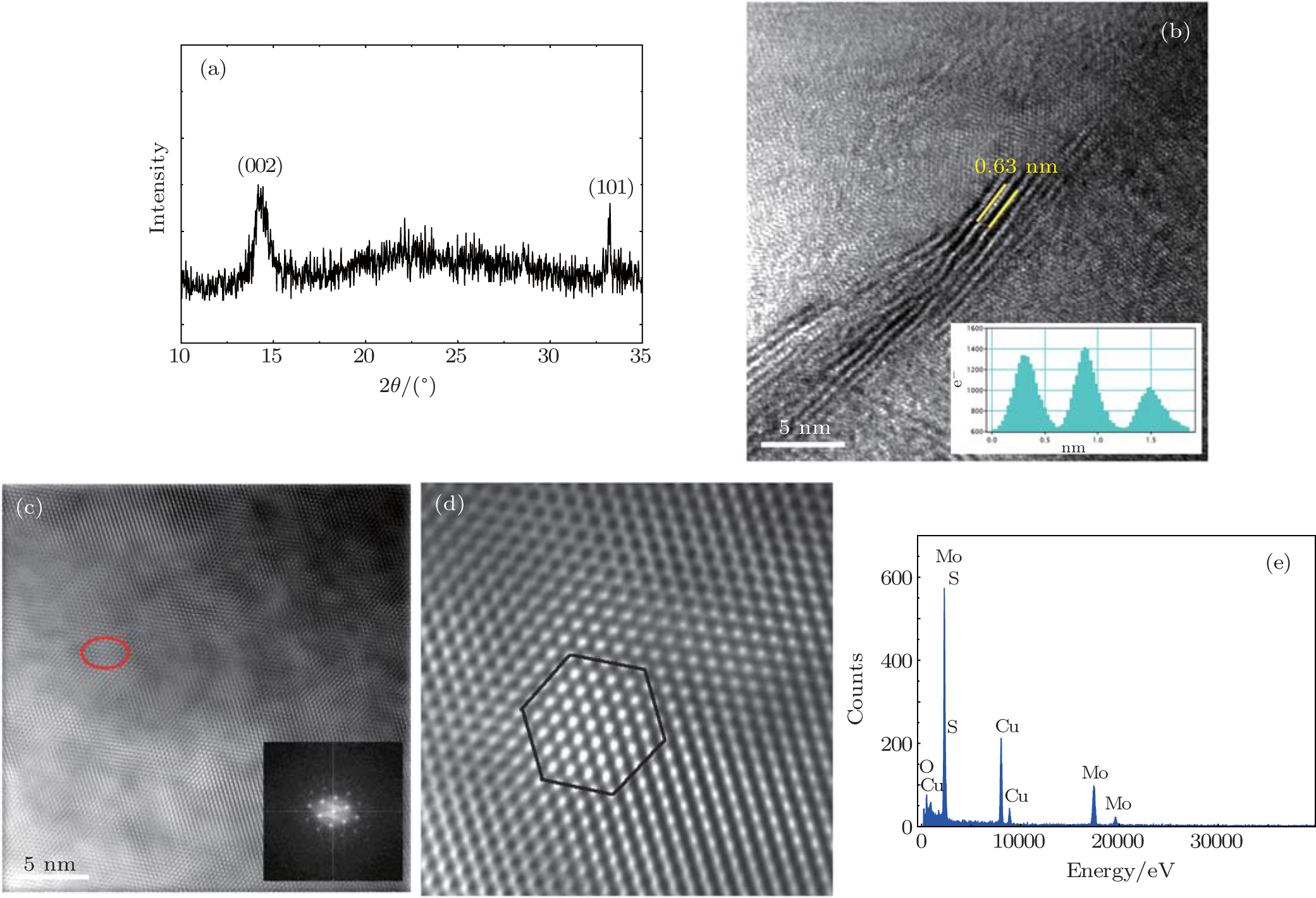
Figure 3(a) shows a typical x-ray diffraction pattern of the thin film acquired using a hot filament chemical vapor deposition method. From the figure, two peaks around 14.3° and 33.2° can be observed. These diffraction peaks in the pattern can be assigned to (002) and (101) planes of standard Molybdenite-2H MoS2, respectively. The observation of the intense (002) peak suggests that, roughly speaking, this material grows in a preferred orientation (002), and may be graphene-like MoS2 layers with a number of layers in the direction of the c-axis perpendicular to the atomic layer,[14] although there is another direction (101) observed. It seems that even though more than one preferred orientation is obtained, the most intensive peak of MoS2 for the (002) reflection indicates a well-stacked layered structure in the film. By using the Bragg equation, the interlayer distance of MoS2 is calculated to be about 0.62 nm, which is in agreement with the theoretical value of d spacing for (002) plane.
In order to investigate the crystal structures in detail, the HRTEM measurement is performed. We prepare the TEM specimen through scratching the surface of the selected area of the film using the TEM grids directly. Sometimes, a wedge-shaped HRTEM sample can be obtained, leading to the “quasi cross-section” HRTEM images. As shown in Fig. 3(b), the structures with stacked layers can be seen clearly. The screwed and crossed morphology are probably due to the mechanical actions during the scratching operations while preparing the TEM specimen. From the inset of Fig. 3(b), the interlayer distance of (002) is measured to be about 0.63 nm from an intensity profile extracted from the HRTEM image, which is in good agreement with the XRD and AFM results. This result also coincides with the order of theoretical value and previous reports for MoS2.[3]
Figure 3(c) shows the plane view of the HRTEM image of the thin film with the atomic resolution exhibiting a clear lattice and the corresponding fast Fourier transform (FFT) of the HRTEM image (inset). We can see well defined spots, indicating a low level of defects. The HRTEM image and the corresponding FFT pattern with [001] zone axis reveal the hexagonal lattice structure with the lattice spacing of (100) planes. The corresponding FFT pattern confirms the symmetrical characteristic features. Figure 3(d) shows the large image of the corresponding area enclosed by the circle in Fig. 3(c). From the figure, a quasi honeycomb-like structure and 6-fold coordination symmetry are observed, corresponding to a 6-fold symmetry spot pattern of ⟨001⟩ reflections.[15] Although the number of defects is small, sometimes grain boundaries can be also observed. The grain boundaries with the feature of honeycomb-like structure with the 6-fold symmetry are also clearly shown in Fig. 3(c).
TEM–EDX pattern of the region enclosed by the circle is shown in Fig. 3(d). From Fig. 3(d), the elements Mo and S are observed. The presence of Cu and C is attributed to the supporter of the TEM grid. The presence of a little O is ascribed to the contamination of the air or incomplete sulfurization. The experimental results prove that layered-structure MoS2 thin films are successfully fabricated.
Fig. 3. (a) A typical XRD pattern for the MoS2 thin film. (b)–(d) HRTEM images of the atomic-layer MoS2 films showing the atomic layers of the MoS2 films and the corresponding EDS spectrum from the region enclosed by the circle of selected area (e). The inset in panel (b) shows the corresponding profile revealing the distance of the interlayer. The inset in panel (c) reveals the corresponding FFT of the HRTEM image. Panel (d) shows the large image of the corresponding area enclosed by the circle in panel (c).
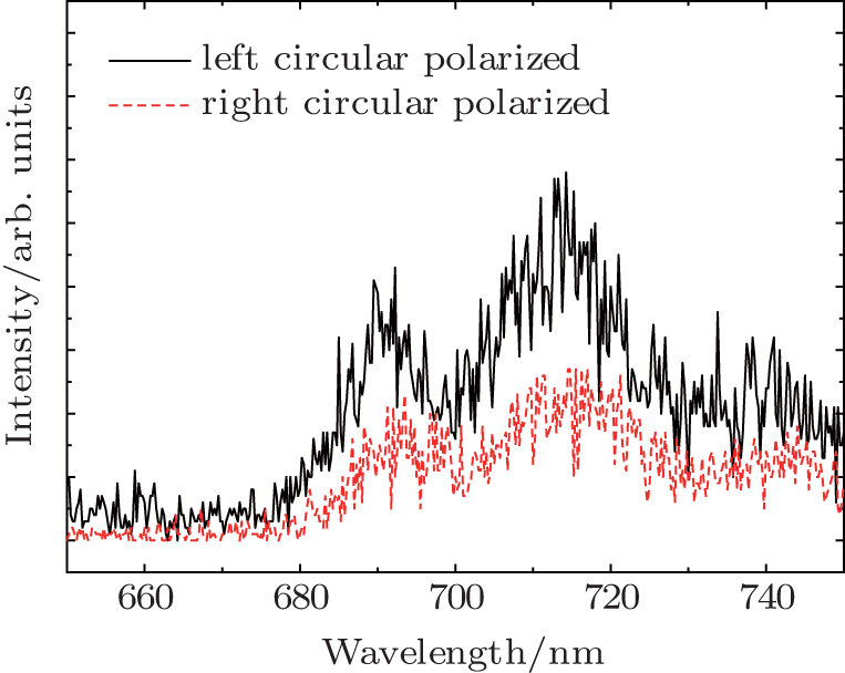
PL spectrum studies offer a route to probe the thickness for an atomic layer of MoS2.[11] It has been reported that PL spectra show strong emission at the A1 and B1 direct excitonic transitions in monolayer crystal of MoS2, which are different from those of bulk MoS2 with the indirect band gap.[11] Under our experimental conditions, it is hard to focus exactly on the zone of the monolayer due to the limit of the equipment, because no micro-PL can be performed. Hence, a larger laser spot is irradiated to cover the atomic layer zone selected. Figure 4 reveals room-temperature PL spectra for the MoS2 ultrathin films under the condition of right-circularly and left-circularly polarized light. That is, they are excited by left-circularly and right-circularly polarized laser at 405 nm, respectively. Both spectra have two emission peaks around 710 nm (1.75 eV) and 686 nm (1.8 eV), which are close to the corresponding values of the direct bandgap of monolayer MoS2.
Fig. 4. Room-temperature circularly polarized components of luminescence spectrum for the MoS2 atomic layers.
In physical concerns, for a monolayer of MoS2, in the Brillouin zone, there exists the direct bandgap between the minimum of the conduction band and the maximum of the valence band at the k and k′ points (two generate valleys). A transition appears from direct bandgap of monolayer MoS2 to indirect bandgap with increasing layer number. The competition between direct and indirect electronic transitions dramatically reduces the PL quantum efficiency.[16] Thus, experimentally the PL spectrum intensity decreases with increasing layer number, until no emission is observed.[11,17] Under our experimental conditions, relatively high intensities of the two peaks of the film suggest that the atomic layer of MoS2, even monolayer in nature definitely exists. Such results coincide with our AFM results. Hence, it is reasonable to assign them to the A1 and B1 direct excitonic transitions, respectively.[1,4,5] On the other hand, at 405 nm, the excitation is well above the A1 and B1 exciton feature, and it should be an off-resonance excitation, that is, less coupling. The red shift of the emission compared with the results in other reports can be explained by a defect trapped exciton mechanism.[4] The energy difference between the two peaks are about 50 meV under our experimental conditions, which is smaller than the reported value of MoS2 by others.[4] This smaller value means a smaller spin splitting energy in our case. Comparing the two spectra, the intensity of the spectrum in the case of right-circularly polarized light is smaller than that of left-circularly polarized light. As is well known, in monolayer MoS2, spin-orbit interaction splits the valence band. The spin projection along the c axis of the crystal is well defined and the two bands are of spin down and spin up in character. Interband transitions at the two valleys are allowed for optical excitation of opposite helicity incident along the c axis. As we do not focus the laser on the monolayer MoS2 but cover the atomic layer area, the observation of the photoexcited carrier density imbalance in different circularly polarized conditions indicates that left and right circular polarization exist in the k and k′ valleys. We know that it is dependent only on the intrinsic band parameters under the assumption of no intervalley scattering.[18] The polarization-resolved photoluminescence spectrum further confirms the presence of the atomic layer MoS2.
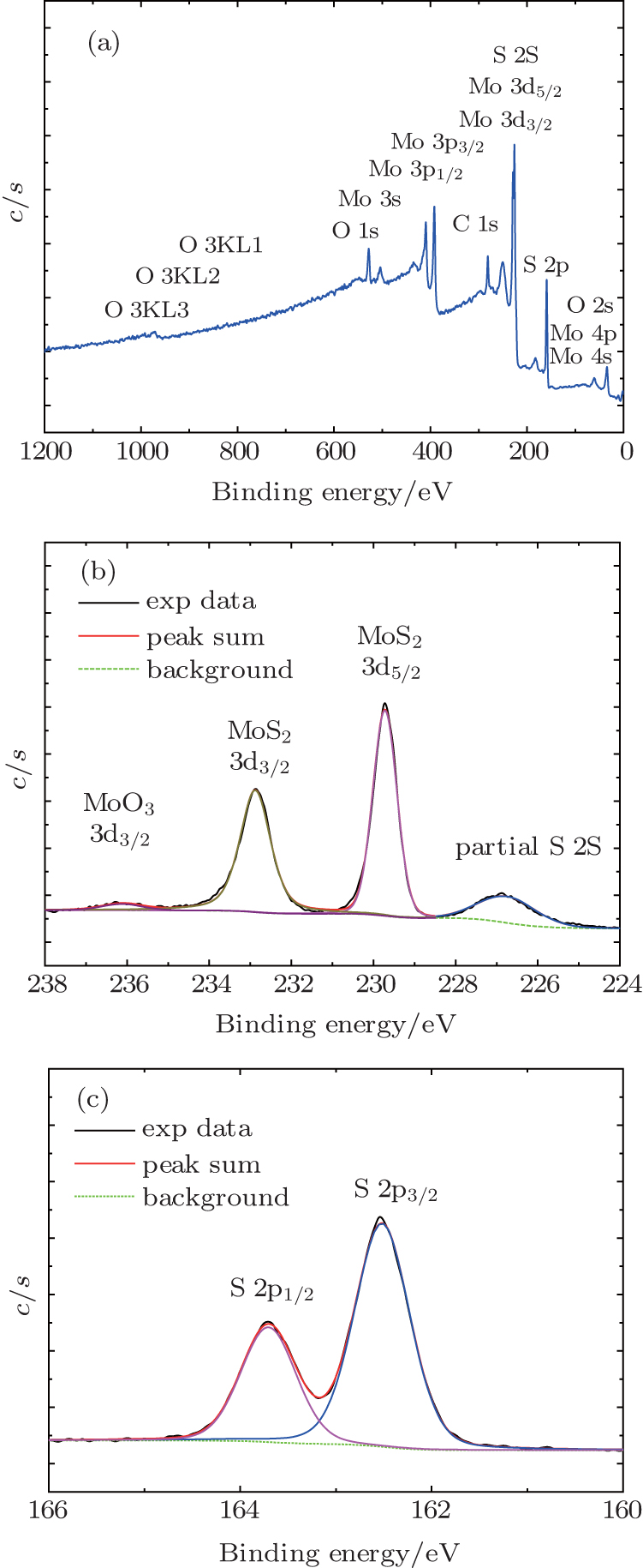
XPS measurements provide further information about the composition, purity and valence states of our film. XPS wide scan spectrum of the MoS2 ultrathin film in a range from 0 to 1200 eV is shown in Fig. 5(a). Only the peaks corresponding to Mo, S, O, and C are observed in the figure, indicating the high purity of our samples. The XPS spectrum of C 1s has been used as an internal reference spectrum,[19] hence the spectra corresponding to Mo 3d core level and S 2p core level of the specimen are calibrated by the binding energy of C 1s as an internal reference spectrum. Then from the spectra, the element atom ratio can be calculated to be about 2.0.
Fig. 5. XPS spectra of the specimen with Gaussian fittings in thinner lines: (a) wide scan spectrum; (b) Mo 3d XPS spectrum; (c) S 2p XPS spectrum.
Figure 5(b) reveals the Mo 3d spectrum and its Gaussian fitting curve. The Mo 3d spectrum can be resolved into four components. The peak located around 229.7 eV is assigned to Mo 3d5/2 spectrum and that around 232.9 eV is for Mo 3d3/2 peak. The binding energy values reveal that molybdenum atoms are in sulfurization state, that is, MoS2. In comparison, there is a small peak around 236.1 eV, corresponding to Mo 3d3/2 in molybdenum oxide. The percentage of molybdenum with oxidation bond in the total bond can be extracted by comparing the corresponding peak areas. Here the peak areas corresponding to Mo bonding in molybdenum oxide are considered completely based on the ionization cross-section from the five-fold degenerate d orbitals, 3d5/2 and 3d3/2. The molybdenum in the oxidation bond is estimated to be about three percent of the total molybdenum bond. Based on our results, the mole ratio of Mo bonding in oxide to that in sulfide is so small that it can be regarded as the contamination from air. Furthermore, the Mo 3d5/2 and Mo 3d3/2 peaks are located with an energy difference of 3.16 eV, which is larger than the corresponding value of metal Mo (3.13 eV) and smaller than the corresponding value (3.2 eV) in MoO3.[20] In addition, a weak peak around 226.7 eV, included in S 2s, is also shown in this spectrum.
Figure 5(c) shows the S 2p spectrum and its Gaussian fitting curve. The peak located at 162.5 eV coincides with the value for S in MoS2. Two peaks which correspond to S 2p3/2 and S 2p1/2 can be observed, respectively. The energy difference between the two peaks is about 1.19 eV, which is larger than the corresponding value 1.18 eV for free sulfur and coincides with that for S bonding in sulfides.[20] The stoichiometry of the ultrathin MoS2 is also studied based on the theory by Baker et al.[21] It is reported that the stoichiometric composition of the MoS2 can be induced from the difference in binding energy between the Mo 3d5/2 and the S 2p3/2 peaks.[21] Based on this theory, the stoichiometric mole ratio of S/Mo is about 2.0–2.1 for the atomic layer MoS2. It seems that it is approximate to the nominal value for MoS2, and this stoichiometric ratio of S/Mo also suggests that sulfur is abundant rather than deficient in our material. We believe that this feature is related to the properties of the atomic layer MoS2 under our experimental conditions. The electrical measurements are also carried out and the results will be published elsewhere.
4. Conclusions
In this work, atomic-layer MoS2 ultrathin films are synthesized using a hot filament chemical vapor deposition method. A combination of AFM, XRD, HRTEM, PL, and XPS characterization methods is used to investigate the crystal structures, valence states, and composition of the ultrathin film areas. The nucleation particles show irregular morphology, while in a larger size somewhere, the films are granular and the grains present triangle shape. The films grow with a preferred orientation (002), that is, the graphene-like MoS2 with a number of layers in the direction of the c axis perpendicular to the atomic layer.[14] The HRTEM images show the graphene-like structures of stacked layers with low density of stacking faults, and the interlayer distance of the plane is measured to be about 0.63 nm. It shows a clear quasi honeycomb-like structure and 6-fold coordination symmetry. Room-temperature PL spectra for the atomic layer MoS2 under the condition of right-circularly and left-circularly polarized light show that for both cases, there are two emission peaks around 710 nm (1.75 eV) and 686 nm (1.8 eV), which are close to the value of the direct bandgap of monolayer MoS2.Relatively high intensities of the two peaks suggest that there exists the atomic layer of MoS2, even monolayer in nature. Hence, it is reasonable to assign these two peaks to the A1 and B1 direct excitonic transitions.[1,4,5] Comparing the two spectra in both cases, the intensities of the peak A1 and B1 in the case of right-circularly polarized light is smaller than that of left-circularly polarized light, that is, valley polarization-resolved PL spectra that have been obtained. The acquirement of the polarization-resolved PL spectra further confirms the presence of the atomic layer MoS2. The XPS measurements indicate that our sample has a high purity aside from some contamination from the air. The binding energy values from the Mo 3d and S 2p core level spectra reveal that molybdenum atoms are in sulfurization state, say MoS2. The stoichiometric mole ratio of S/Mo is about 2.0–2.1 for the atomic layer MoS2. It seems that it is near the nominal value of MoS2. Furthermore, the value of the stoichiometric ratio of S/Mo also suggests that sulfur is abundant rather than deficient in our material, which coincides with the AFM result. We believe that this feature is related to the properties of the atomic layer MoS2 under our experimental conditions. The electrical measurements are carried out and the corresponding results will be published elsewhere.


 , Song Yang1, Xie Xiao-Qiang1, Li Yuan1, 2, Qian Zheng-Hong2, Bai Ru2]